Hi Ostripper
greetings thanks for replying i now have all the components ready
to start this project
warm regards
andrew lebon
Any help you need with layout , please ask.
I am starting with a small pair (4-OP devices) for my secondary hi-fi amp , I
am sure a "monster" 20 device amp will work with proper local decoupling and layout.
OS
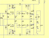
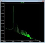
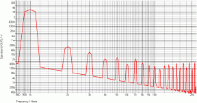
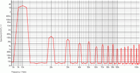
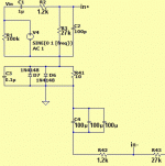
I think you need few more gain stages, it should sound lot better!VAS loading -
Look at the comparison below:
Amp #1 - has no loading. LF gain is 78db. it's bandwidth (UG-unity gain) is 390Khz , and the lead
compensation (C6) had to be increased to 15pF to keep -103 degrees margin.
Less than 1db extra gain at 20K available for feedback. This combined with
the extra distortion of a larger C6 adds up to .01% THD20.
Amp #2 - Loaded by the 2- 100K resistors .LF gain is only 66db, the margin goes out to 618K
the gain at 20k is 32db! 32- the 26 of the amp leaves 6db extra.
Besides at much better .002% THD20 , C6 can be reduced to 10p to give the same -103 degree margin.
H3 also decreases with the loading.
Conclusion - loading sacrifices gain at lower frequencies for more gain at
the higher ones. 1/5th the THD at 20K is the result. TMC does the same
work in a typical "blameless" topology.
This is also why you see the THD plots of most amps " reach skyward"
at 25 to 30k - no extra gain above 20K !
PS-this is why Sansui used the loading resistor.
OS
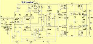
GLA AMP
Hi Ostripper
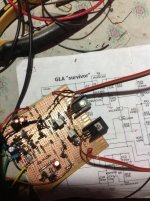
greetings just finished the GLA amp i made it on a dot board pcb
copper side facing upwards and amp worked on first power on SOUND QUALITY
is fantastic superb just need little guidance to make the HIGH POWER version
many thanks for this wonderful schematic and all the hard work you have done to stimulate the amp in lt spice need your help in pcb layout single sided i just want to finish the high power version
warm regards
andrew lebon i will upload picture shortly
Hi Ostripper
greetings just finished the GLA amp i made it on a dot board pcb
copper side facing upwards and amp worked on first power on SOUND QUALITY
is fantastic superb just need little guidance to make the HIGH POWER version
many thanks for this wonderful schematic and all the hard work you have done to stimulate the amp in lt spice need your help in pcb layout single sided i just want to finish the high power version
warm regards
andrew lebon i will upload picture shortly
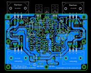
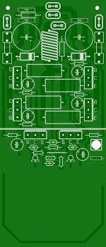
PCB for GLA
...... one day work and voila......just someone compare schematic with layer , and I will post ,the rest in black /white ,silk screen......
Regards ,Alex
...... one day work and
voila......just someone compare schematic with layer , and I will post ,the rest in black /white ,silk screen...... Regards ,Alex
Attachments
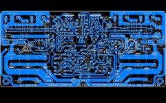
Last edited:
couldn't wait to design PCB. some ugly dot board work this amp really sounds good
Warm Regards
Andrew Lebon
See .... I do not pick the "duds".
The design is a "survivor" 1981-2013 !This IS NOT your standard blameless or leach. Faster slew (fast amp)!!
Alex MM - you rock...
Could you do a MT200 device 4 OP layout ?
- just the 2 -470uf PS decoupling + the driver decoupling 22u.
What I'll do is layout my prototype .... you "prettify it" ,
the layout of this amp is more critical than blameless-EF2's.
My study of the sansui layout leads me to believe this.
I'll have to look over your layout very carefully , this one I will build to
A/B with the "badger".
OS
Last edited:
the layout of this amp is more critical than blameless-EF2's.
My study of the sansui layout leads me to believe this.
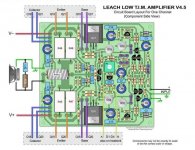
Also , study the famous "Leach" amp layout (attachment 1).
The triple OP is much more prone to inductance feedback.
Keeping the high current rails,the OP bus, and the NFB path FAR away from the
predrivers and input stages is crucial.
(Attachment 2)
Notice ....
A - Inductor is all by itself (alone and far away
).B- Output bus and NFB takeoff point are isolated.
You notice ... by the time the NFB takeoff reaches (C) , there are
no current pulses and then I drop the voltage with the lead comp.
/feedback resistor before I cross the predriver base traces (D).
At (E) voltage is low with just uA's of current.
Below the point where I stopped
, the small signal stages wouldbe very isolated from any current/inductance.
There is method to the "madness" ..... the leach layout adheres to these
same rules religiously.
OS
Attachments
Andrewlebon , follow the leach amp layout criteria and use the "tweaked"
new schematic (below).
This one is final , just extend the output section of my layout ( add as many
as you want) You might also mount the drivers (njw0302/0281) on the
main heatsink. With 8 pair MJL 21193/4 , driver SOA will be approached.
PS - you might want to use the recommended mje340/350 for predrivers as well,
for a "Frankenstein amp"
HA ! Just imagine how stressed a single pair of poor little mje15032/33's would
be in the typical DIYA "blaster amp".
BTW , what was your DC offset??
OS
new schematic (below).
This one is final , just extend the output section of my layout ( add as many
as you want
) You might also mount the drivers (njw0302/0281) on the main heatsink. With 8 pair MJL 21193/4 , driver SOA will be approached.
PS - you might want to use the recommended mje340/350 for predrivers as well,
for a "Frankenstein amp"
HA ! Just imagine how stressed a single pair of poor little mje15032/33's would
be in the typical DIYA "blaster amp".
BTW , what was your DC offset??
OS
Attachments
Last edited:
Hi Ostripper
greetings thanks for replying i am excited to see this thread progressing and
many thanks to Alex for his pcb design the sound quality is amazing treble so clear and soft bass also very nice i will pursue this project till the end and follow all your expert advice
warm regards
andrew
greetings thanks for replying i am excited to see this thread progressing and
many thanks to Alex for his pcb design the sound quality is amazing treble so clear and soft bass also very nice i will pursue this project till the end and follow all your expert advice
warm regards
andrew
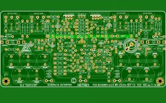
Rev 2.0 for Sanken transistor
Hi Pete ,
My second attempt, to layout same schematic ,but with Sankens OP transistors.
Not easy at all, to put in line ,all transistors , I mean OP I try another layout , when I will find some free time , this weekend was enough for me......
Thanks andrewlebon , kind as usual ....
Regards ,Alex
Hi Pete ,
My second attempt, to layout same schematic ,but with Sankens OP transistors.
Not easy at all, to put in line ,all transistors , I mean OP
I try another layout , when I will find some free time , this weekend was enough for me......Thanks andrewlebon , kind as usual ....
Regards ,Alex
Attachments
Hi Pete ,
My second attempt, to layout same schematic ,but with Sankens OP transistors.
Not easy at all, to put in line ,all transistors , I mean OP
Thanks andrewlebon , kind as usual ....
Regards ,Alex
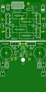
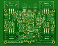
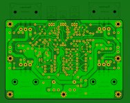
That is better ! I see most of the layout rules are in place.
I reconsidered .... the MT200 sankens are too "dang" big !!
Best go with TO-3P (MT-100)
(Below - Attachment 1) is what I had in mind....
1. The asymmetrical power rail layout , like the "badger".
Most of the REAL expensive "audiophile" amps have this layout style.
2.The PS off to one side , the coil on the other.
3. For a small amp like this 4 OP one , the drivers can be on their own heatsinks - the original Sansui used class B drivers (I'll show you that change
in .... attachment 2).
Heatsink(s) should be just a flat piece of metal spanning the 2
drivers.
4. Large pads, fat traces - most will be toner transferring this (I will).
5. 153mm X 76mm layout ... USA is inches for FR-4 (6 X 3).. this is how they sell it here.
Look at the layout below....
Alex - I love your work - it is art in the physical world
.PS - class B for the drivers changes nothing , not even the Distortion components (attachment 3). ....... Nice !!
Andrewlebon , I would be cautious separating the driver board - or using cable
interconnects. Some on the forum have even had slight problems with
this approach with EF2's ! Running JUST the outputs on a separate board
would be better , but then you would still need to cable the NFB return.
(I've done this...)
OS
Attachments
A few sims with a single output pair.....
Works good ... huh!
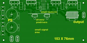
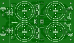
I finally decided on what power supply and layout scheme I want.
Similar to Jen Rasmussin's leach layout for the amp.
.....And a modified CRC for the power supply.
Both will be done with BOM's , Schema's , and printable board artwork.
(below 1/2)
It takes more than a day to properly layout an amp like this. I spent MORE
than a day just researching triple OP stages and similar layouts on this forum.
I split the amp's grounds into "dirty" (OP stage/ drivers/predivers) and "clean"
(regulators / input ground)
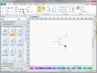
I also have "EDRAW MAX" (attachment 3) .... professional .
I'll also make a build guide for this amp with it's history , operation , and
modifications.
PS - this amp will be class A drivers , have 4 pair njw0302/0281's from my badgers.
Output as driver - robust !
OS
Attachments
Last edited:
Nice work so far from both schematic designers and pcb designers.i will follow the progress of the thread .i have 4 pairs of mjl21193/94 sitting for many years and i would be glad to use in a stereo amp like this with 2 pairs for each channel. keep up the good work.
by the way ,ostripper the final pcb in its finall form will look like post 53 or post 55?
by the way ,ostripper the final pcb in its finall form will look like post 53 or post 55?
Mine will be #55. Best way.
Might be able to fit all on a 76mm X 153mm.
OS
ok.i am looking forward for the pcbs..
- Home
- Amplifiers
- Solid State
- GLA (good little amp) "survivor"