Attempt at offering an explanation for the new symptoms. (DC at higher volume)
When the current demand on the negative rail is high the voltage/current at pin 8 (mute) drops below its threshold and mutes the chip. When the current demand returns to the positive rail the chip is unmuted. If this is what is happening then the chip will output the positive signal and mute a large portion of the negative signal.
If this is the problem, then how to fix it: Rm, Cm, load, bypass caps, PSU caps, connect Rm to PSU and not to the bypass caps, voltage/current transformer, add a diode in series with Rm.
Your photo does not show the PSU, the bypass caps or how they are connected.
I have only seen this in simulations and have no idea what it sounds like, what the measurements look like or even if this is actually the problem.
.
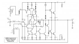
Interesting idea, Mark Whitney. Meanwhile, maybe it will help visualization to have a complete circuit. Posted is the circuit from the TI data sheet. Components from Figure 1 are edited onto the chip schematic on page 7 without any changes.
Of course, the data sheet shows only a partial schematic, TI doesn't give away all the goodies. But you gotta go with what you got.
.
Attachments
Last edited:
Thanks Mark and bantsnake, looks like that may have been happening.
My gainclone is badly jinxed Now a new problem. Last night after coming back from a colleague's farewell, I decided to use a thicker wire for all the DC power going to the chips. I may have done something wrong because the bulb in series was glowing bright. I discovered either a stray short because of some solder or some incorrectly connected pin (am trying hard to recall, but cannot). I resoldered some wires and the bulb in series was very dim. Then I had both channels connected and tested the output voltage without any speakers. One channel had good output, whereas the second one did not have any.
I was then testing it in isolation. There are no shorts, powering up keeps the power supply running. DC offset is around 0.7mv. There is no AC output with input signal present.
I tested by shorting the pins 9 and 10 of LM3886, still the same thing. I have a new chip, tested the resistance between different pins, and the one not working and the new one are pretty much similar in terms of resistance.
Is there a way to test the IC? I googled a lot and could not find anything. Again, there are no shorts, no 0 resistance between any of the pins, resistance between output and pin 3 is finite (not open circuit).
If anyone has a test circuit, pls provide the details.
Thanks
My gainclone is badly jinxed
Now a new problem. Last night after coming back from a colleague's farewell, I decided to use a thicker wire for all the DC power going to the chips. I may have done something wrong because the bulb in series was glowing bright. I discovered either a stray short because of some solder or some incorrectly connected pin (am trying hard to recall, but cannot). I resoldered some wires and the bulb in series was very dim. Then I had both channels connected and tested the output voltage without any speakers. One channel had good output, whereas the second one did not have any.I was then testing it in isolation. There are no shorts, powering up keeps the power supply running. DC offset is around 0.7mv. There is no AC output with input signal present.
I tested by shorting the pins 9 and 10 of LM3886, still the same thing. I have a new chip, tested the resistance between different pins, and the one not working and the new one are pretty much similar in terms of resistance.
Is there a way to test the IC? I googled a lot and could not find anything. Again, there are no shorts, no 0 resistance between any of the pins, resistance between output and pin 3 is finite (not open circuit).
If anyone has a test circuit, pls provide the details.
Thanks
Hi All,
I plugged the circuit back in, and checked the status of it.
Present situation is this, experts please help.
I see no output still at pin 3. DC offset is 0.7mV (with or without input signal)
Pin 8 is at 3V wrt ground. Pin 4 is -41V. Which means 38V is dropped across Rm(20K), calculation tells me current draw is ~1.9mA. I think it should be >0.5mA. Still no output.
What can we conclude from this? Resistance between output pin and pin 4(metal heatsink) is 2.7Kohms or something (not 0).
Thanks,
Mohit
Also, I checked some other things.
I disconnected Rm, and voltage at Pin 8 wrt to ground was 0.
I connected Rm in series with my multimeter, and the current draw was 1.7mA
I checked the pins of the chip. Each pin is not touching any other pin and has 0 resistance between the pin base and pin on the board.
With Rm removed, DC output at pin 3 is exactly 0mV. With Rm connected, it is 0.6-0.7mV. No AC output.
Thanks,
what is the Difference between these two voltages?................. DC voltage on pin 9 and 10. I have -3.4mV on 9 and -2.7mV on Pin10 if this helps.................
What is the output offset?
Are they the same?
How does an LTP input work?
And from that last question with your answer you will see how the input LTP ends up with a -ve voltage on the +IN pin.
Last edited:
Hi Andrew,
Because I was having all the DC offset issues, I had redone the layout (as you have seen the picture of). In this, the audio and power ground are the same. What this means for the circuit is that the pin 7 is proxy for the audio ground, which is later connected to audio ground.
I tried hundreds on things, one of which was removing the 1uF cap from input. When I did that, I noticed that the resistance between the audio in and ground fell to 0.4 or so ohms. I was shocked, thought the resistor was shorted or something. I put in a new 33K resistor, and still the same thing. Then I put the 1uF cap back on, and the resistance became 4K, still nowhere near the 33K. Could you explain to me what is happening here?
Thanks much,
Mohit
an opamp and a chipamp generally have a two transistor input stage.Andrew, the difference is around 0.7mV, and is the same as output offset.
Sorry don't understand what LTP means...could you pls clarify?
Thx
They are arranged as a Long Tail Pair.
The inputs to the opamp/chipamp can be at any voltage level from just above the -ve supply rail to just below the =ve supply rail.
BUT the really important part of every differential input opamp:
The DIFFERENCE between the inputs is multilplied by the gain and appears at the output.
the difference between -3.4mVdc and -2.7mVdc is 0.7mVdc.
The DC gain of the chip amp should be ~1times (+0dB)
The Output voltage should be 0.7mVdc * 1times = 0.7mVdc.
The +ve Input is lower than the -ve input therefore the output should be -ve with respect to Audio Ground.
Is it + or -?
Sounds like what you have built is not what you have on paper.Hi Andrew,
Because I was having all the DC offset issues, I had redone the layout (as you have seen the picture of). In this, the audio and power ground are the same. What this means for the circuit is that the pin 7 is proxy for the audio ground, which is later connected to audio ground.
I tried hundreds on things, one of which was removing the 1uF cap from input. When I did that, I noticed that the resistance between the audio in and ground fell to 0.4 or so ohms. I was shocked, thought the resistor was shorted or something. I put in a new 33K resistor, and still the same thing. Then I put the 1uF cap back on, and the resistance became 4K, still nowhere near the 33K. Could you explain to me what is happening here?
Thanks much,
Mohit
Draw it out carefully and check every component value and every connection.
Confirm this on the paper schematic.
Then you maybe know what you have built.
At the moment it looks like you don't have a clue !
- Status
- This old topic is closed. If you want to reopen this topic, contact a moderator using the "Report Post" button.
- Home
- Amplifiers
- Chip Amps
- Gainclone DC on output