You are right.
Do you have any topology description for reference for class BD?
I am thinking to make it.
Check the 5-6 page of the attached file.....
Attachments
Check the 5-6 page of the attached file.....
Thanks
Unfortunately attachments removed
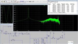
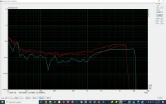
IMD test 35Vp-p
Very impressive IMD, that promise high end sounding amp, I was busy with one also with poles to get lower distortions, but time is a problem here, but now winter is coming and work less I go start with the amps again.
regards
This is a good compendium of abilities at work.
The residual magnetic field from the inductor is picked up as a tiny square wave by signal traces and components. A close ground plane (as in 4+ layer PCB) attenuates that by 20~30dB. 5cm of distance has a similar 20~30dB attenuation effect (measured for the leakage field of a 25mm OD toroid core). A balanced modulator can increase rejection by 40dB. Flipping the spatial plane of a single axis-coil can provide over 40dB of attenuation (less for toroids as radiation is not single axis).
Why not an output inductor with the leakage field oriented in a spatial plane different to the plane of PCB in which modulator resides? This will certainly help with multi-channel application. Otherwise distance is the only solution for minimizing alterations in noise floor, in low volume operation, between modules.
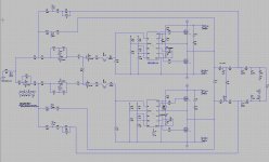
Now this revision of the printed circuit board is being finalized. The board is 4-layer.
Of course, differential circuitry is used.
Thank you for the concretization of the interference.
unfortunately, I had to reduce the size of the PCB which produced a deterioration in the parameters .But, nevertheless, THD + noise <0,002%.
At the moment it seems to me that the greatest level of interference is radiated by the midpoint of the FET, and precisely the charging currents of parasitic capacitances.
Since I use high-speed comparators it is also very important to use high-quality output filter capacitors. The presence of even 30nH of parasitic capacitor inductance is inadmissible. In fact, all high-capacity polypropylene capacitors can not be used
In short, there are many nuances.
Hi all experienced class d friends.
Sorry I do break in so suddenly with this question.
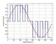
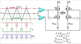
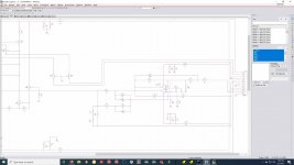
I have tryed to experiment somewhat with (bi-)unipolair modulator but get when I input a circuit into ltspice strange results, see picture. on the output bridge I get to much, and that give uge shoot through stuff.
output needs as in picture two, maybe I do have to offset the input sinusoidal signal? as say the example bookwork it is not. on the output comparators I get only positive signals, maybe wrong somparators. the sinousoidal is one inverted to comp input, use two comparators.
what I doing wrong. because is seems very simple but see not the fault, wel I do see it, I have 2 to much signals on output, and think the inputsignal needs offsets. thanks in advance.
Sorry I do break in so suddenly with this question.
I have tryed to experiment somewhat with (bi-)unipolair modulator but get when I input a circuit into ltspice strange results, see picture. on the output bridge I get to much, and that give uge shoot through stuff.
output needs as in picture two, maybe I do have to offset the input sinusoidal signal? as say the example bookwork it is not. on the output comparators I get only positive signals, maybe wrong somparators. the sinousoidal is one inverted to comp input, use two comparators.
what I doing wrong. because is seems very simple but see not the fault, wel I do see it, I have 2 to much signals on output, and think the inputsignal needs offsets. thanks in advance.
Attachments

By adjusting the operation of the output stage, it was possible to reduce the distortion below 0.001% to half the power.
Little long ago but did you respond on mine question?
I have in the meantime do some learning, and it seems that with this multilevel adjusting of the switching stage is important.
I have also did more levels for to see what happens, promissing,but more parts,..
regards
Attachments
I think that such a multi-level option has no prospects. Since the reason is not clear. Why complicate the system if it does not bring an improvement in its performance?
Optimization of switching output transistors seems to me a more promising way to obtain the necessary parameters.
Although Bruno demonstrates a different path. In purifi, he increased the loop gain.
Optimization of switching output transistors seems to me a more promising way to obtain the necessary parameters.
Although Bruno demonstrates a different path. In purifi, he increased the loop gain.
It is more for learning some more about class d, I do like with no feedback, such a multilevel is then a idea to get lower distortion, further effect is the multiplying effect of the carrier into the Mhz who simplify low pass and eventual feedback.
I agree this one is a little overkill, but it is a nice learning project and build and test it for to see what it does, That is why we here right, neat projects.
I am still busy with the circlotron autobias, I need a discrete low distortion opamp for that.
For class D the three level self oscillating is very nice, do double carrier and have feedback (afcourse otherwise it does not oscillate) it has post and prefeedback, it does work nice with postfeedback that way what normally is so difficult.
That one is more simple and I go build these some day wgter the cpb milling machine is build and ready.
regards
Hey Sous,
Thanks for this thread. I ended up building a single ended half-bridge version where an integrator (opa1462 with sallen key filter) feeds a discrete modulator directly. Power stage is controlled using the cheap irs2011. I clamped the modulator input to the integrator non inverting input using red smd leds with low capacitance. I have yet to add additional passive poles to the modulator input but here is the current results at 30watts into a 6ohm load with 45v-+ rails. DC offset 11mv. Sound card THD floor is ~0.0015%.
Apparently I don't know how to attach images. Anyways, THD @ 1k 0.002% THD @ 6k 0.005%
Thanks for this thread. I ended up building a single ended half-bridge version where an integrator (opa1462 with sallen key filter) feeds a discrete modulator directly. Power stage is controlled using the cheap irs2011. I clamped the modulator input to the integrator non inverting input using red smd leds with low capacitance. I have yet to add additional passive poles to the modulator input but here is the current results at 30watts into a 6ohm load with 45v-+ rails. DC offset 11mv. Sound card THD floor is ~0.0015%.
Apparently I don't know how to attach images.
Anyways, THD @ 1k 0.002% THD @ 6k 0.005%
Last edited:
Hey Sous,
Thanks for this thread. I ended up building a single ended half-bridge version where an integrator (opa1462 with sallen key filter) feeds a discrete modulator directly. Power stage is controlled using the cheap irs2011. I clamped the modulator input to the integrator non inverting input using red smd leds with low capacitance. I have yet to add additional passive poles to the modulator input but here is the current results at 30watts into a 6ohm load with 45v-+ rails. DC offset 11mv.
Thanks for this thread. I ended up building a single ended half-bridge version where an integrator (opa1462 with sallen key filter) feeds a discrete modulator directly. Power stage is controlled using the cheap irs2011. I clamped the modulator input to the integrator non inverting input using red smd leds with low capacitance. I have yet to add additional passive poles to the modulator input but here is the current results at 30watts into a 6ohm load with 45v-+ rails. DC offset 11mv.
Hey Kees52,
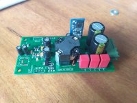
I need to figure out how to add images to posts but yes it was designed in Orcad using a home built 2layer pcb with a separate daughter board for for the input stage. Uses T130-2, FDP2572's, has temperature, over current, over/under voltage protection and using 3"x4"x1.5". To keep cost and part count down I went with single ended which allowed the use of only 1 dual channel op amp. I went with the opa1642, one channel is the sallen key 2nd order filter combined with a passive first order filter that feeds the second channel that is used as an integrator. Sallen key has a gain of 2.4 and integrator has a gain of 12.2 giving a total gain of roughly 29db. Currently switches at 530khz when idle... still need to play with additional passive poles.
Also THD wasn't my only goal with this amp.. My main goal was to get below 0.01% across the board at high output. Other goals include very low noise, low idle current and not crazy expensive. The opa1642 is so very quiet and the total idle current on 45v+- rails is only 55ma.
Kees52, looks interesting... Have you built one yet?
Last edited:
Something to do with how i tried to attach the first images .
Anyways, its not the same way Sous was going about doing his amp but this thread got me started. I did try feeding the comparator from the first stage and using the integrator to only correct but in the end this approach achieved better results and clamping using LEDs made it easy. I did try clamping with 1n4148s but they conducted too early and would need three in series to work correctly (waste of board space).
Note the values for the sallen key wont make sense until you know there is also a passive 1st order in series on the main board, values are 1k, 3nf. Also note the reason why the caps on the integrator are different are to try to keep it easy on the op amps output. I had designed this around the TL072 at first and will change the values since the OPA can handle more load.
.Anyways, its not the same way Sous was going about doing his amp but this thread got me started. I did try feeding the comparator from the first stage and using the integrator to only correct but in the end this approach achieved better results and clamping using LEDs made it easy. I did try clamping with 1n4148s but they conducted too early and would need three in series to work correctly (waste of board space).
Note the values for the sallen key wont make sense until you know there is also a passive 1st order in series on the main board, values are 1k, 3nf. Also note the reason why the caps on the integrator are different are to try to keep it easy on the op amps output. I had designed this around the TL072 at first and will change the values since the OPA can handle more load.
Attachments
- Status
- This old topic is closed. If you want to reopen this topic, contact a moderator using the "Report Post" button.
- Home
- Amplifiers
- Class D
- full differential UcD modulator with extra integrator