Hi Andy,
Click share at the right, it will show "Anyone who has link can view" and a change link at the right. Click change and check Allow Anyone to Edit and save. That will do it !!
Once you close the Group Buy, revoke the edit access so that you will be the only can change again.
Cheers,
Click share at the right, it will show "Anyone who has link can view" and a change link at the right. Click change and check Allow Anyone to Edit and save. That will do it !!
Once you close the Group Buy, revoke the edit access so that you will be the only can change again.
Cheers,
Yes,
I see your point, however, I would also imagine that any ripple would be a greater problem on the input stage.
It's not a big deal to add some cap positions on the ouput boards although it will mean running a ground connection that wasn't previously required.
The F5 is relatively insensitive to ripple on the rails, as long as it is the same on the rail ends of the MOSFET source resistor (R18) and the JFET drain resistor (R5). This is why case must be taken to minimize AC currents in the path between the rails on output board and the input board. You might allow for caps on both boards and people can experiment to see what works best.
Yes,
I see your point, however, I would also imagine that any ripple would be a greater problem on the input stage.
It's not a big deal to add some cap positions on the ouput boards although it will mean running a ground connection that wasn't previously required.
Thinking more about this issue, there might be an advantage putting putting everything beyond the JFET drains on the output boards: R5, P1, and C21(R6, P2, and C2 for the other rail). Perhaps the all of the cascode circuitry could go there too, and then no rail voltages are needed of the input board. The only concern then is to minimize induced currents in path from the JFET drains to the output boards.
If this were done, then the input board becomes absolutely trivial and it would make sense design one for a balanced or X-ed version too.
I need to analyze this some more and do some SPICE simulations of the noise behaviour of this approach.
Hello
I do not want a mono block. Still I need two PS board?
Please let me know why? Do I need 2 power transformer to?
Thank you
Greetings gabor
Read the manual first. Page 14
http://www.firstwatt.com/pdf/art_f5_turbo.pdf
Thinking more about this issue, there might be an advantage putting putting everything beyond the JFET drains on the output boards: R5, P1, and C21(R6, P2, and C2 for the other rail). Perhaps the all of the cascode circuitry could go there too, and then no rail voltages are needed of the input board. The only concern then is to minimize induced currents in path from the JFET drains to the output boards.
If this were done, then the input board becomes absolutely trivial and it would make sense design one for a balanced or X-ed version too.
I need to analyze this some more and do some SPICE simulations of the noise behaviour of this approach.
Sounds like it would be best if Toe was to put everything on one board .... Hey wait a minute ..
")
Hello labjr
Thank you for letting me know these important information!
Now I understand why required 2PS board and probably 2 transformer to.
OK I do take the two power supply boards at the order but still I go with one PS board.
Why?
Because I use max 36VDC rail voltage!
I have a 1KVA 30V transformer (new Plitron) I will use for these project. If the Aleph4 works with one PS with 36V rail voltage must be OK these amp to.
I will use a soft start on the transformer primery that will help a lot.
Only question remain if I use lower rail voltage can I bias the amp all the way in Class A mode? I do not want Class A/B amp with such a investment.
Also I do not want to invest in new power transformers. I have several new transformer.
Do it has any bias adjustment option?
Thanks one more time.
Greetings Gabor
Hello for f5 in the version where we increase only the tension. We have to reshape the food(supply) I be understandable can one take simply two bridge(deck) rectifiers no diodes RIPE(MATURE), and apply the plan of the food(supply) 16 x 15000µf instead of 10000µf as to the plan posted in turbo F5, for the food(supply) thank you
Hello for f5 in the version where we increase only the tension. We have to reshape the food(supply) I be understandable can one take simply two bridge(deck) rectifiers no diodes RIPE(MATURE), and apply the plan of the food(supply) 16 x 15000µf instead of 10000µf as to the plan posted in turbo F5, for the food(supply) thank you
You can use 15000uf capacitors instead of the 10000 with no problem.
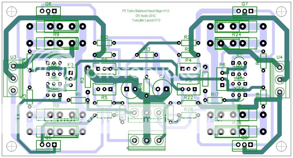
UKtoecutter, I urge you to "find space" between the components!
For example you have the power resistors that go to the Mosfets right next to each other.
They need space to breathe.
The layout is packed into the center. Why?
Small and tight is nice, but there is no reason not to use the horizontal space on the board.
Fatter pads can be used on the small jFets by making the pad pattern triangular rather than in-line.
etc...
Use the space, Luke, use the space!
_-_-bear
Hello
The 30V is AC before the bridge.
At Class A I get 36VDC. I do not understand your question? Usually the primery what you connect to the wall. 120V or in Europe 230V..
Secondary what you get from the transformer (or I'm wrong)
So the rail voltage it would be 36VDC under Class A load.
Greetings Gabor
The 30V is AC before the bridge.
At Class A I get 36VDC. I do not understand your question? Usually the primery what you connect to the wall. 120V or in Europe 230V..
Secondary what you get from the transformer (or I'm wrong)
So the rail voltage it would be 36VDC under Class A load.
Greetings Gabor
Hello
The 30V is AC before the bridge.
At Class A I get 36VDC. I do not understand your question? Usually the primery what you connect to the wall. 120V or in Europe 230V..
Secondary what you get from the transformer (or I'm wrong)
So the rail voltage it would be 36VDC under Class A load.
Greetings Gabor
I was asking if it was before or after the rectifier, I wrote it wrong.
acording to the f5t paper if you want 36v you'll need 27v ac before the rectifier.
30v ac will give you 40v after the rectifier.
Hello, MASantos,
Gábor was right.
For example, in my F4 those 1KVA/2x25V toroids gave me 30,7V DC.
Between the caps, on the shunt resistors drops 0,3V, so before it has 31V DC.
So the ratio ACVx1,24=DCV.
If I remember correctly as if Papa would have said something similar somewhere.
(What a nice alliteration, huh?)
One toroid supply two channel. These two channel dissipate approximately 480W.
Best,
Gyuri
Last edited:
- Status
- This old topic is closed. If you want to reopen this topic, contact a moderator using the "Report Post" button.
- Home
- Amplifiers
- Pass Labs
- F5 Turbo Circuit Boards