OK fellas.
I've tried to take on board all your comments.
Please see revised layout.
Board is now 300mm x 50mm
I've tried to take on board all your comments.
Please see revised layout.
Board is now 300mm x 50mm
An externally hosted image should be here but it was not working when we last tested it.
OK fellas.
I've tried to take on board all your comments.
Please see revised layout.
Board is now 300mm x 50mm
An externally hosted image should be here but it was not working when we last tested it.
IMO traks to long and different lenghts
can you (I mean I would) first place trak for speaker output on one side of board (pins don't have to line up can be bent back or forward a bit.
That would be the track you ear and the one carring signal 3 mm maybe more (the more the better)
then do the rest working over that.
Work on one side first and mirror on other side (+ and - )
If you ask nicely Zen (we all love him realy) is realy quik in posting nice picies of Papa lay out (mind bogling simple and elegant).
Another dumb question How much heath came out of the Diodes?
Maybe litle sinks for those do
I'm not sure I understand what you're saying.
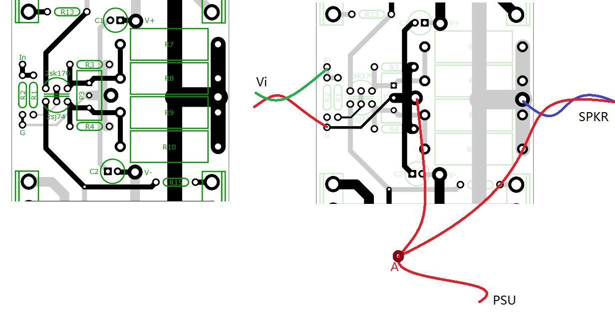
The output is on the top of the board between Q4 & Q6 presented on a two position Phoenix connector (Bear in mind this is just one channel).
The input is on the bottom of the board.
I appreciate what you're saying regarding track lengths but I am keen to to get plenty of seperation between the output devices to spread heat along the whole length of the heatsink (that's why tracks are long). Dissipation is what I'm after.
The Diodes are on the board edge in order that they can be mounted on the heatsink.
Andy
Sorry at work so I have to describe
Keeping all your mosfets as they are on top of picture as we are looking at it.
Draw the track going to the speaker as a straight line connecting the 4 drains
Once you got that do the rest.
The positive and negative suply conect more or less the same pins on the 2 separte side of board.
Draw one side then copy/ mirror to other
Last edited:
No need of a speaker return on the pcb. Can be wired at main star ground, leaving input ground clean.
At least separate ouptut ground path from input ground path.
look at current flowing through R7, R8, R3 when output is near positive rail.
I still don't get you, sorry for bothering you. I know the speaker output ground will return to the common ground at point A as stated. But still, i still don't understand why you mention that the signal ground and decoupling ground cannot end at the middle ground on the PCB before connecting to point A. Maybe my english understanding is a bit poor that i have misunderstood you.

See if the following attachment correct:
Sorry, i was mixing a bit with Uktoecutter layout.
What i mean is: it is preferable to choose a star point on the pcb and return decoupling caps their own way.
On your, input resistors return and decoupling caps return use a common path.
But maybe i am splitting hairs into pieces as the path is so short and trace is doubled.
Your understandig is certainly better than my english.
Last edited:
bksabath
OK, taken on board your comments and I've tried to make as symmetrical as possible.
A bit awkward with the long thin board but hey, never mind.
Andy
OK, taken on board your comments and I've tried to make as symmetrical as possible.
A bit awkward with the long thin board but hey, never mind.
An externally hosted image should be here but it was not working when we last tested it.
Andy
Hi Andy
Well now the most important track is well sorted.
Don't you think ?
I have one tought regarding the source diodes.
They only conduct when current get up so V drop across the resistor increase over a certan limit could those do better on theyr own litle sinks?.
I will try your aproach and then the other way.
Kroompst
I was doing nicely with the board and program crashed.
Silly me no saves for jonks.
If sometink is bound to happen it will strive to happen as soon as possible.
So got to start againg.
Tanks 6L6 yes they do question is how much and how often.
How often is how often current demand get above the point at which V drop across sources get up to certain point so not much while amp idle.
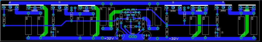
Here is the first one.
There is a lot to tidy up and I would stager the pins of Mosfets and Diodes so to save corners on the tracks like on sketch.
Just for the record I am not saing that is beter or worst than any Is just my way to pluck a Duck (I like cats so there you have it)
There is a lot to tidy up and I would stager the pins of Mosfets and Diodes so to save corners on the tracks like on sketch.
Just for the record I am not saing that is beter or worst than any Is just my way to pluck a Duck (I like cats so there you have it)
Attachments
It's amazing how much yours is similar to mine Bksabath.
Mine is still alfa, need to check it still but this layout can be expanded easily....
also working on a version with transistors on right and left....will post if there is interest.
Attachments
Last edited:
It's amazing how much yours is similar to mine Bksabath.
Mine is still alfa, need to check it still but this layout can be expanded easily....
also working on a version with transistors on right and left....will post if there is interest.
I like yours the most now... it's simply neat and good!
Would be interesting to see a rectangular board with outputs on both sides since about the best heatsink available in the states is from Heatsink USA and the deepest one they make is only 10 inches.
I did noticed the manual mentions mono blocks. Would it work well to have all the N channel devices on on side and the P channel devices on the other heatsink?
I did noticed the manual mentions mono blocks. Would it work well to have all the N channel devices on on side and the P channel devices on the other heatsink?
since about the best heatsink available in the states is from Heatsink USA and the deepest one they make is only 10 inches.
If you use a single sink, yes, but if you are willing to make a frame to hold more than one together, you have infinite depth. FWIW, the hifi2000 cases, at 400mm or bigger are all multiple heatsinks.
I did noticed the manual mentions mono blocks. Would it work well to have all the N channel devices on on side and the P channel devices on the other heatsink?
That's more of an issue with the layout of the PCB than anything else. It's one one the reasons Peter Daniel makes his PCB as small as possible, it actually gives you more choices with how things are mounted and gives more flexibility in what kind of sinks you use.
It's amazing how much yours is similar to mine Bksabath.
Mine is still alfa, need to check it still but this layout can be expanded easily....
also working on a version with transistors on right and left....will post if there is interest.
I like it beter than mine.
Yes cascodes is what I have at the moment and that is going to be the way I am going to make it as well.
2 toughts
1) I may put a couple of resistors in series with P3 last time I tried that I fried the Jfets.
2) I already have MYF5 with most of the bits in place apart from the diodes I wonder how much different the F6 is going to be.
It's amazing how much yours is similar to mine Bksabath.
Mine is still alfa, need to check it still but this layout can be expanded easily....
also working on a version with transistors on right and left....will post if there is interest.
Ooh. That is a work of art. I am shamed!!!!
Back to the drawing board to do an imitation
It has always humored me how many people clone the FirstWatt designs using the long skinny boards. If you have ever seen the FirstWatt heatsinks in person, or a really good photo of them, you see why the boards are arranged like that.
But... with the heatsinks that are available to the DIY community, however, a smaller and more rectangular board is highly advantageous. You can still make a highly symmetrical board, but IMO smaller is actually better.
The one i posted is for the community....221 x 36 mm...but i do agree with you, I prefer the more rectangular ones for my heatsinks, that is why i'm working on the other version with the active power devices, 4 each side. 87 x 127...
It's amazing how much yours is similar to mine Bksabath.
Mine is still alfa, need to check it still but this layout can be expanded easily....
also working on a version with transistors on right and left....will post if there is interest.
CeeVee,
Can you check your P3 connections.
I think they're going to the wrong side of the input FET's (i.e. should be S on the 170 and D on the 74).
Andy
Last edited:
Thanks Andy,
I've corrected that mistake...doing rest of board and will post later after full review.
It's source on both ! not Source and Drain...
Of course (which is why I've just made a hasty modification to my schematic!!!)
- Status
- This old topic is closed. If you want to reopen this topic, contact a moderator using the "Report Post" button.
- Home
- Amplifiers
- Pass Labs
- F5 Turbo Circuit Boards