Hi
Not sure what is causing your issues but you may be having some sort of transient voltage being passed on from the source.
The zeners are connected anode to anode (or cathode to cathode, both work fine) and the the two remaining electrodes are connected across the 100k input resistor, or from input node to ground. This prevents excessive voltage spikes from destroying the input FETs.
Also remember to keep the input shorted when adjusting bias and for a few hours after. Once the DC conditions are verified stable, you can connect speakers. I use a RCA plug with a single soldered wire across the terminals. It's indispensable for setting initial conditions of all amplifiers.
I cannot imagine that your grounding would be causing your failures, but the zeners will help at least the gate of the Jfets.
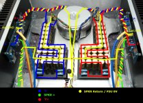
Aesthetics look great, even down to the well twisted pairs in very many locations.1-3 : The attached image show the internals, the PSU 0V is not showing twisted in this image but it is, following the PSU V+/V- wires.
4 - So I would be much better off eliminating the bridge between negative outlet and rather join 0V directly between the two cap banks? And connect with Chassis GND using a CL60 in series?
But you broke the cardinal rule.
All the current coming out of the PSU (Source) MUST RETURN to the PSU/Source. That pair of Flow and Return wires MUST be close coupled, or better twisted.
Since only alternate halves of the +ve current Flow in the +ve supply wire and the complementary alternate halves of the -ve current Flow in the -ve supply wire, these two wires must become part of the twisted triplet.
Shame the Amp PCB does not have the three solder pads beside each other. (=bad design by someone who does not understand current Flow and Return !).
Last edited:
I would recommend that you hot test the amp for a few days and cycle through cold to hot at least a couple of times after finalising the output bias. Temporary bias voltage test wires out through a ventilation hole. Both wires through the same hole !!!!.................Also remember to keep the input shorted when adjusting bias and for a few hours after. Once the DC conditions are verified stable, you can connect speakers. I use a RCA plug with a single soldered wire across the terminals. It's indispensable for setting initial conditions of all amplifiers................
...This prevents excessive voltage spikes from destroying the input FETs...
If excessive voltage spikes are the culprit:
Since it is only the SK170's that have failed here, would that indicate that these spikes originate from one of the two cap banks? I would assume that both the SK170/J74 would be subjected to damage if the problem was "global"
inserting/removing the input plugs may be the problem.
especially since no RF attenuation is fitted as standard.
When I have briefly tested with singal RCA have only been hooked up with power off. However the initial run-in adjusting bias have been with inputs open. I will short these for the next round.
But you broke the cardinal rule.
All the current coming out of the PSU (Source) MUST RETURN to the PSU/Source. That pair of Flow and Return wires MUST be close coupled, or better twisted.
Since only alternate halves of the +ve current Flow in the +ve supply wire and the complementary alternate halves of the -ve current Flow in the -ve supply wire, these two wires must become part of the twisted triplet.
See revised diagram, have I got it right?
Attachments
Last edited:
It's better, but just to understand current flow - the central point is where all the high currents will return to. So the speaker must be wired here, as well as the two 0V connections from the bridge rectifiers.
It's important that the ground going to the two boards MUST be drawn from the same point, not from the individual rectifiers. I understand you are probably doing this to keep the wiring symmetrical and concluding that short wire lengths must be better. They are, but the first rule is to respect currents.
You should use a thin length of wire to connect the 0V for the boards if you are using a single point off-board for speaker return. If using the board 0V for the speaker output (the thicker track of the 'T' on the board carries the speaker current), then use the same AWG wire as you have used for power.
It's important that the ground going to the two boards MUST be drawn from the same point, not from the individual rectifiers.
I have assumed that as long as the 0V shared contact somewhere along the chain (Currently @ bridged negative speaker outlet) I was good, apparently that is not the case as I have not considered current

So basically what I am adviced to do:
Lift GND using CL60 making a single physical point.
Directly connect both cap bank 0V rails to this point.
Directly connect speaker negative lines to this point.
Directly connect PCB GND to this point using thin wire.
Last edited:
I find it much easier to think about all the current pairs. Wire them up first.
Then look to see if any connection is missing.
There will be three missing connections in a two channel amplifier.
Left Signal Ground to Left Power Ground.
Right Signal Ground to Right Power Ground.
Power Ground, OR PSU Zero Volts, to Chassis. This last can go in various locations. Read Leach, he recommends experimenting with moving from the Zero Volts to Chassis to the input RCA sockets to Chassis for some builds.
But do ALL the cable pairs as close coupled or twisted first. This gets the loops very small and helps prevent an inadvertent loop through a distant wire that you had forgotten about.
Pairs for left speaker, right speaker, left input, right input, AC mains, secondary from transformer, mains AC to the fuse if separate from the IEC socket, the LED indicator, the heatsink Thermal switch, the DC detect if fitted, etc .....
A triplet for the dual polarity PSU.
Thank you Andrew.
I pulled Q1-Q6 off the bad amp yesterday and tested these and apparently they are still all good. My tester detected the correct parts and showing expected values. I started fresh with a new PCB which now is fully populated, only lacking the cables which will be moved over this evening.
I will redo the grounding scheme also, in a day or two I should be able to test it again.
If you do all the pairs FIRST, you will find that most of the "grounding" is sorted................. I will redo the grounding scheme also, in a day or two I should be able to test it again.
"grounding" is a misleading word. Most are actually the RETURN of a Flow and Return PAIR.
That's why doing ALL the pairs first is so simple. It completes ALL the RETURNS and leaves very little to complete the final wiring.
May I ask of an opinion of the following layout?
This is what I have planned after taking the advice offered here, joining Return between the two PSU banks (red dot, yellow line).
PCB 0V (marked Aud.GND) follow V+/V- line and track back to star ground. Speaker Return also connect at star point as do PSU 0V.
Given the layout of the hardware, is this a good approach?
Attachments
Last edited:
That does not look right.
Start at the transformer secondary. Blue and yellow are close coupled.
After the first two "T" junctions the yellow and the blue become separated. The yellow after the "T" junction has to follow the second part of the blue and becomes the twisted pair.
How does the red get across to twist with the blue and yellow? This then forms the twisted triplet.
The speaker return and the speaker flow get from the speaker terminal to near the PCB as a twisted pair, then they split and sepaarte.
The flow and return must remain close coupled until they eventually get back to the Source of the speaker current, i.e. back to the PSU blue & yellow and PSU Red & yellow.
Last edited:
That does not look.
As in electrically "incorrect/potensional hazard" or as "not ideal" noise-wise?
Quick question:
While adjusting the initial bias on one side should this affect offset on the other side ( a few mV) ? Since the PSU load increases, voltage will drop a little and affect the circuit on the untouched side?
After being left to cook over night bias and offset was solid, heat sink luke warm. Increased the bias to 0,420V and left to cook while I am at work. Offset is easily being managed.
Q3/Q4 Vgs=3,9V
Fingers crossed that my issues now have been sorted
Last edited:
I described the blue and yellow routes and where they went/should not go.As in electrically "incorrect/potensional hazard" or as "not ideal" noise-wise?
Am I wasting my time?
Andrew - I certainly hope not and if you feel that way please accept my apologies.
However what your "does not look right" statement related to was unclear to me, hence my follow-up question. While my english is decent it is only my 2nd language, maybe I am not communicating my intent clearly either.
The internal layout options available to me is partially given by the amb boards (fixed design) , the cap bank (my design) and location of the input/output/ground points.
Per your advice I have close-coupled/twisted all pairs as much as possible but at some point they will split up. I am unable to spot a better/simpler wiring arrangement given the limitations of my layout arrangement.
I could as done previously let PCB GND (Yellow) terminate at the rectifier 0V but it was also adviced to make these return to the common point.
My primary objective right now is to make my amp work after experiencing a couple of setbacks, my main change this time around is that speaker return isnt going to the amp boards anymore but directly to the common point. And both rails are now directly connected to eachother, not shared via the longer 0V lines coming from both amp boards.
Last nite I went through the steps validating the integrity of the wiring, voltages were good, bulb went out and initial biasing went without issues - so as far as I am conserned the advice given and the path taken, appear to be sound. Building this amp is ment to be a learning experience, the next one will hopefully become even better. Any advice or thoughts given to me during this process have been appreciated.
Last edited:
- Home
- Amplifiers
- Pass Labs
- F5 power amplifier