I don't think so.Could this problem be due to bad / discontinuous thermal contact of the thermistor(s) with the mosfet after the first thermal cycle?
The thermistor adjusts the output stage bias current by changing it's own resistance in response to a temperature change.
I can't see how that blows a semiconductor.
hello halari,
either I'm confused from your graphic or your circuit has no proper mag(main audio ground) which should be made from each a positive and a negative output of your rectifierbridges and should be connected to at the capbanks output.
see firstwatt f5 manual
greetings
either I'm confused from your graphic or your circuit has no proper mag(main audio ground) which should be made from each a positive and a negative output of your rectifierbridges and should be connected to at the capbanks output.
see firstwatt f5 manual
greetings
Can you measure the Vgs on the output MOSFET on the good and bad channels? This should tell you whether the problem is at the input or the output.
Also see if temporarily disabling the current limiting helps.
If I was you I would bias it to about half the recommend bias for a day or so before giving it full beans. I normally do that to verify that the circuit is OK. I use even less, just 150mA for a couple days at least.
Measured voltages:
Good side:
V(in) 49.9V
Q3 P-channel 24,1V over pin 1 & 2, 0V over 2 & 3.
Q4 N-channel 24.1V over pin 1& 2, 14-18V over pin 2& 3
Bad side:
V(in) 49,9V
Q3 and Q4, measured 24.9V over all pins.
(this side have had P1/P2 set to zero ohm measured over the 2k2)
Thanks for the tip on slow start, will adhere to that
")
hello halari,
either I'm confused from your graphic or your circuit has no proper mag(main audio ground) which should be made from each a positive and a negative output of your rectifierbridges and should be connected to at the capbanks output.
see firstwatt f5 manual
greetings
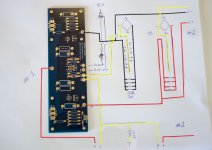
I have highlighted the MAG in yellow shown on the attached image. Hope this is more understandable. If its dubious let me know!
Attachments
Last edited:
Halla Halair: R'e u shure your termal pads are correct and the protecting paper is remooved?
Hei
Keratherm used, mosfets had no paper backing.
The mosfets are testet for continuity to chassis ground with R15 measured (resistance of the CL60 used to tie Audio GND to Chassis GND)
pins 1, 2 & 3 are what? Source, Gate, Drain?Q3 P-channel 24,1V over pin 1 & 2, 0V over 2 & 3.
The voltage across/over pins 2 & 3 looks very suspicious for the "good channel" !!!!!
Just one question. Probably ok but maybe worthwhile mentioning anyway.
Are the yellow 0V of + and - psu boards connected? Drawing does not show it and suggests that channel 2 has speaker - connected to gnd of channel 1.
Are the yellow 0V of + and - psu boards connected? Drawing does not show it and suggests that channel 2 has speaker - connected to gnd of channel 1.
Measured voltages:
Good side:
V(in) 49.9V
Q3 P-channel 24,1V over pin 1 & 2, 0V over 2 & 3.
Q4 N-channel 24.1V over pin 1& 2, 14-18V over pin 2& 3
Bad side:
V(in) 49,9V
Q3 and Q4, measured 24.9V over all pins.
(this side have had P1/P2 set to zero ohm measured over the 2k2)
Thanks for the tip on slow start, will adhere to that
I have highlighted the MAG in yellow shown on the attached image. Hope this is more understandable. If its dubious let me know!
The voltages and the drawing both look suspect.
The two rectifiers are not shown as being joined together to create the ground at all. To have a split rail supply You need a common point, it seems that this is not present in your drawing.
Can you confirm this?
Also, look at the F5 manual and use the exact same nodes for voltage readings. Replace the voltages with you actual measurements and then we can see the issue.
You may need to dial up the bias pots a bit on the non-working channel to get some measurements...
Just one question. Probably ok but maybe worthwhile mentioning anyway.
Are the yellow 0V of + and - psu boards connected? Drawing does not show it and suggests that channel 2 has speaker - connected to gnd of channel 1.
Not directly to each other, I believe they are connected via PCB GND/speaker negative terminals.
Rectifier #1 0V is connected to PCB 1 GND
Rectifier #2 0V is connected to PCB 2 GND
GND of PCB 1 connect to speaker negative terminal 1
GND of PCB 2 connect to speaker negative terminal 2
Negative terminal 1 & 2 are brigded and terminated to chassis gnd after the CL60 thermistor.
If 0V on rectifier 1 & 2 was directly connected would it not create a ground loop if the rest of the wiring was kept intact?
@AndrewT : will report back pin out and re-measure voltages.
pins 1, 2 & 3 are what? Source, Gate, Drain?
The voltage across/over pins 2 & 3 looks very suspicious for the "good channel" !!!!!
I measured over wrong pins previously.
Vgs (voltage over Source and Drain pin, pin 1&3 ref pin out for IRFP9240/240)
Good amp Vgs Q3=3,9V and Vgs Q4=4,0V (Bias = 0,580V)
Bad amp Vgs=0 for both Q3/Q4. ( to be expected as P1/P2 are currently set to zero ohm measured over the 2k2 resistors? )
Q3 & Q4 Vgs of 3.9V & 4V looks good.
Thank you Andrew for your time and reply.
The voltages and the drawing both look suspect.
The two rectifiers are not shown as being joined together to create the ground at all. To have a split rail supply You need a common point, it seems that this is not present in your drawing.
I initially missed your reply, my apologies.
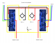
I have made a new drawing showing the current wiring configuration.
I believe the common PSU point is made where the two speaker negative terminals bridge, sharing a CL60 connected to chassis GND. If this is a poor way to achieve Audio GND let me know.
Both boards read 52,4V (under no load, both channels off) over their V+/V- terminals. Both boards have played music. In other words the PSU works and have GND? Yet I have 3x 2SK170's that are blown and likely a 4th after one board went to zero when cooking a week ago. (all 2SJ74 prior to this checks OK)
It occured to me that the current bridged negative outlets could cause trouble if one side goes bad, inserting voltage over negative outlet on the good side?
BTW voltages on the good board:
Vgs = ~4,0V on both IRFP's (measured over the two outer pins, Gate/Source pin)
Voltage over the 2k2 resistor = ~4,4V with bias set to 0,580V.
On the bad side I havent dialed it up yet but will do so tonite and measure. Then I will pull out the presumably defective SK170 and assemble a new board.
Attachments
Last edited:
Vgs looks fine, so does the drain resistor reading. Will wait for your progress report. I would send both ground commons to both boards from the PSU itself. This would means creating a single ground common, just like the ref schematic of power supply. This provides the smallest current loop for the PSU return. If the ground are separate on both boards, you can send 4-wire PSU connections, but keep both boards identical.
If yoiu are regularly blowing the 170s, you might try a zener on the input just for additional safety. 5.1v units should be fine, you need two connected back to back. Maybe there is a problem upstream.
If yoiu are regularly blowing the 170s, you might try a zener on the input just for additional safety. 5.1v units should be fine, you need two connected back to back. Maybe there is a problem upstream.
If yoiu are regularly blowing the 170s, you might try a zener on the input just for additional safety. 5.1v units should be fine, you need two connected back to back. Maybe there is a problem upstream.
Such as? (learning mode ON)
First time it failed both SK170's went belly up at the same time when playing music. No other damaged components found (but all Q1-Q6 on both sides were replaced)
Second time one SK170 blew, smoking R3 (the other board wasnt connected)
Third time with new SK170 & R3 the same bad side went cold after initially setting bias with offset=0,00V without issues. As in amp left on, good readings on both sides, let to cook, one hr later the bad board was cold. The other board still going strong.
Could you please elaborate on the zeners?
Last edited:
PSU power to PCB:
the return current from one PCB does not follow the route of the Flow current.
The three wires of the dual polarity power supply must arrive as a close coupled (or twisted) triplet and then connected to the PCB solder pads.
PCB to Speaker:
The two wires of the Flow and Return from PCB to the speaker must be a close coupled (or twisted) pair.
Then repeat this wiring arrangement for the other channel.
When you do the triplet to BOTH PCBs you will find that the Zero Volts provides the near zero ohms connection between the two channels. This is your first and compulsory PCB to PCB ground link.
There must not be any other near zero ohms ground links between the channels.
The inputs will have a remote link between the Sources signal grounds. Use D.Joffe solution of inserting a resistance to attenuate the loop current below audibility.
Your diagram does not follow that !
PSU power to PCB:
the return current from one PCB does not follow the route of the Flow current.
1 - The three wires of the dual polarity power supply must arrive as a close coupled (or twisted) triplet and then connected to the PCB solder pads.
2 - PCB to Speaker:
The two wires of the Flow and Return from PCB to the speaker must be a close coupled (or twisted) pair.
3 - Then repeat this wiring arrangement for the other channel.
When you do the triplet to BOTH PCBs you will find that the Zero Volts provides the near zero ohms connection between the two channels. This is your first and compulsory PCB to PCB ground link.
There must not be any other near zero ohms ground links between the channels.
4 -Your diagram does not follow that !
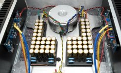
1-3 : The attached image show the internals, the PSU 0V is not showing twisted in this image but it is, following the PSU V+/V- wires.
4 - So I would be much better off eliminating the bridge between negative outlet and rather join 0V directly between the two cap banks? And connect with Chassis GND using a CL60 in series?
Attachments
I have made a new drawing showing the current wiring configuration.
I believe the common PSU point is made where the two speaker negative terminals bridge, sharing a CL60 connected to chassis GND. If this is a poor way to achieve Audio GND let me know.
All the speaker current is running through the PCB, not good practice, high current pulses can damage the track.
The two rectifiers each feed a bank of capacitors, the farthest 'end' capacitor on each bank should be linked together to create the common ground point (yellow connections on your drawing), this common ground is where the speakers return should be connected, the ground connection from the amp PCB's are also connected here, plus the CL60 link to chassis earth; connect the input ground to the PCB.
- Home
- Amplifiers
- Pass Labs
- F5 power amplifier