Hi All,
First, thanks for the help the other night. Got the traffo and PS board all wired up. Bulb tester lit up, then went out; good. Measured ~28V output from the PS.
Mounted the output devices to the heat sinks. Checked for continuity, none; good. Connected output devices to boards, connected boards to PS. Dialed back the pots. Turned the amp on. Bulb tester lit up, then went out; good.
Started to adjust the pots to show a few millivolts across R7 & R8. Could not get voltage to show up at R7 on the right channel, no matter how much we turned the pot. R7 & R8 on the left board showed voltage, as did R8 on the right board.
Any suggestions as to what may cause this? Bad P1? Bad Q5?
Check all solder joints properly, as well as pot orientation.
If not, check the JFET operation (you may need to remove the output device from the board). Keeping wiper at max resistance should show voltage across the drain resistor, and with power off there should be a change in the resistance when you turn the trimmer. (not 0-5k, more like few ohms-1.5k). Remember to set the trimmer back to zero ohms before powering up and connecting the output device.
If none of this works, your output device may be bust. I start at the output device, check gate drive (G-S) on the output device pins. If there is about 2.8V and no voltage across the associated source resistor, the output device is dead, and if there is no gate drive it is a problem with the front end or a cold/loose solder somewhere in the chain.
Sorry for not posting part numbers as there are multiple versions of schematics and boards.
Figured it out... Someone soldered in two P-channel JFETS instead of one P and one N. Doh!
BTW, we're trying the 2SJ103/2SK246 combo instead of the 2SJ4/2SK170 combo. Are there any changes we need to make either to the circuit or to the biasing procedure when using this combo?
BTW, we're trying the 2SJ103/2SK246 combo instead of the 2SJ4/2SK170 combo. Are there any changes we need to make either to the circuit or to the biasing procedure when using this combo?
I'm Baaack... Happy New Year's Eve to all...
I tried piggy-backing the J103s and K246s as ZM suggested, and I'm able to get within biasing range. Unfortunately, with the FETs I have (10 each Ns and Ps) I can't get good N/P matches (Ns range from 4.5-4.8 Idss, while Ps range from 3.2-3.7). As a result I couldn't equalize the readings across R7 & R8 to .59V, and the best offset I could get was ~1.7V.
Short of busting the already strained budget by buying the LS FETS, are there any suggestions for getting a working amp with what I have? I could get the LS FETS, but would have to wait some time before doing so. I've read a lot of the related threads, but applying that info this build is a bit beyond my newbie capabilities...
Thanks for all your help so far. I'm learning (I think), but slowly...
You could try 2 x 4.8 (= 9.6mA) in parallel to match up 3 x 3.2mA (= 9.6mA) in parallel (don't overheat the pins) - maybe not exactly what is specified but will give you a closer current match - will need to alter the pot a bit to obtain the 0.59V, but it's a possibility with your existing devices ...
Idss for the input FETs is not the only thing that matters in a F5 (or similar) circuit.
The open loop gain, and hence the amount of feedback and hence closed loop distortion depends, among others, on the transconductance of those devices.
The cost of a pair of 2SK170/2SJ74 or equivalent is a very small fraction of the cost of your entire build.
So I do not follow the logic of saving USD20 or so but sacrifice performance in the process.
Unless the look is more important than the sound .....
You can get matched Toshiba's from Spencer.
No need to use LS FETs.
Store FET Audio | Hi-End Audio Projects
There are circuits which works well with the other JFETs such as 2SK246/2SJ103.
But they are designed from scratch to work with those devices.
A good example is the headphone amp from Ric Marsh.
http://www.diyaudio.com/forums/headphone-systems/211394-marsh-headphone-amp-linear-audio.html
If you want the same performance, there is simply no substitute for 2SK170/2SJ74, IMHO.
Patrick
Quick question: I'm building the PSU V3 (cviller build); unfortunately for R1-R8 I've only got these big-*** 0.47R resistors that dissipate 5W. They won't fit next to each other without touching. I'd either have to mount them in a low-high-low-high configuration, mount them alternatingly over/under the pcb or make use of the optional spaces for resistors and leave an empty spot between. over/under doesn't seem right because it complicates mounting the pcb and I'm not comfortable with thermal dissipation. What would you guys do (all answers are good except 'order smaller resistors that dissipate 3W and fit)?
The build is for a standard F5, power supply a 500 VAC with 2 18V secondaries, the power board will have 8x 15000 microF 50 V caps.
Thanks and happy new year.
BTW: I'm slowly reading through this thread, at page 170 now so in case this has been answered already, have mercy..
The build is for a standard F5, power supply a 500 VAC with 2 18V secondaries, the power board will have 8x 15000 microF 50 V caps.
Thanks and happy new year.
BTW: I'm slowly reading through this thread, at page 170 now so in case this has been answered already, have mercy..
May I ask for some guidance? I have tried searching but to no avail and the DiyAudio Store BOM-link isnt working...
I have the cviller F5 V3.0 boards and original BOM list from the NP manual.
Problem - the BOM do not correspond to v3 board layout. Nor does it list component value on the board. Could some one please guide me to where I can find a matching part list?
I might be missing the obvious but I am getting crosseyed") . Please...
. Please...
I have the cviller F5 V3.0 boards and original BOM list from the NP manual.
Problem - the BOM do not correspond to v3 board layout. Nor does it list component value on the board. Could some one please guide me to where I can find a matching part list?
I might be missing the obvious but I am getting crosseyed
. Please... I would suggest a slightly different way to go about assembling your parts list -
Print out a full circuit diagram with the component values on them
Then write down the values on a separate list by the diagram numbers (ie: R1, R2, etc) and then separate the different resistor power ratings
This makes you chase around sorting out the different components and where they are situated - gives a far better understanding about the pcb and layout and particularly makes you more aware of the ground wire connexions
Then you go looking for your parts - Elfa gave just about everything you need, apart from the jfets (see Patrick's link to Spencer Cheung in HK), and maybe the European transformers from Poland - I think the rest you can get from Hannes (h_a) - not sure about the heatsinks and case, maybe Italy ...
I have the parts obtained already (Spencer and Hannes both used) including the PCB boards from DiyAudio Store. BOM used for purchase is from the NP build manual.
I also have the cabinet in house, Modushop/Italy 4U/400mm Dissipatio including a 400VA 2x18VAC toroid. Resistors etc are also on hand.
However, the PCB layout and part number was changed from v2 to v3 so the list do not any longer correspond, the store BOM isnt updated yet (been so for a while)
This is where I am stranded as I am unable to find a good guide for populationg the v3 board with confidence
Last edited:
The new refdes numbering matches the F5 turbo, so look at that and I am sure your confidence will increase.
Thank you cviller, do you have a link that I can use to make a cross reference chart?
I find it easiest to work from the schematic - BOM have a tendency to go old and smelly in short amounts of time.
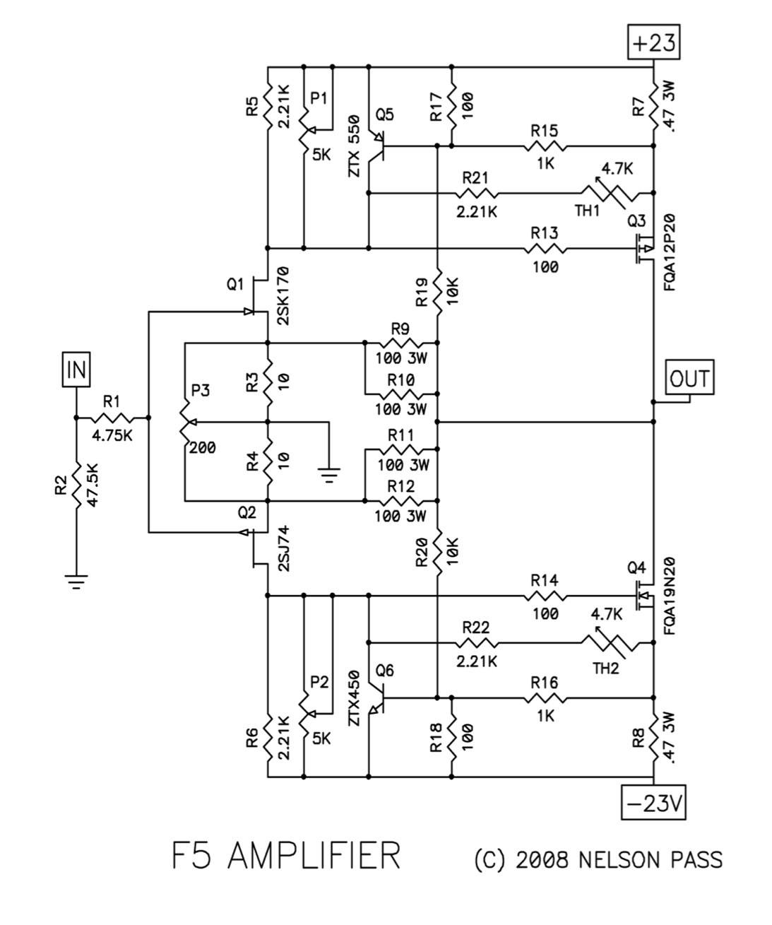
This schematic is from the F5T article and should match the latest version of PCB.
P3 should be set to it's mid-point -- equal resistance from pin 1-2 and from pin 2-3. The track isn't 200 ohm long exactly, so measure. As for setting it to find the distortion spectra you like the most, you can just count turns in either direction as you adjust it... but keep notes!
R19, R20 in the latest schematic are part of the limiter circuit.
The orientation of the Toshiba K170/J74 or K370/J108 match the orientation drawn on the silkscreen. The silkscreen for Q5, Q6 is shown genderless, but the Collector, Base, Emitter are labeled so you can determine proper orientation - the reason for this is that the most common transistors used in the position, the ZTX and the BC, have different pinouts.
Last edited:
- Home
- Amplifiers
- Pass Labs
- F5 power amplifier