jackinnj said:The plot which I published depicted the P-channel replaced. I then replaced the N-channel as well and the result is the same -- still peaks at around 500kHz
The closest I've got is to get a 1 dB peak at about 800 KHz.
Personally I wouldn't bother with anything at that value, but yours
appears to be a little more severe.
Looks to me like you'll have to break down and install 2 compensation
caps. one across each of the 50 ohm resistors on the feedback loop.
(By the 50 ohm I mean the parallel 100 ohm resistors.)
Suggested initial value would be .0022 uF.
Re: Complementary MOSFETs
Hi Patrick
Did you ever try these devices in the design?
I would be interested to know how they faired
Cheers
Tim
EUVL said:
While waiting for the Fairchild EU group buy, which is forcast now from Digikey to be 10 weeks (!!! ), we have got a few Toshiba 2SK1530's / 2SJ201's to play with.
The pdf attached plots drain current vs Vgs referenced to bias point, with both values inverted for the P-device to ease comparison. The bias current is 2A for both FETs, Vgs is 2.38V for the N-device, and -2.30V for the P-device. Transconductance at bias is about 4.5 S.
Red line is 2SK1530; light blue crosses are 2SJ201. It was a hell of a job to make the two sets of data visible from one another in excel.
A picture says a thousand words.
Patrick
Hi Patrick
Did you ever try these devices in the design?
I would be interested to know how they faired
Cheers
Tim
Prototype is 60% ready (PCBs, matched FETs, heatsinks, mechanical parts, ....), just waiting for PRP resistors to arrive from the US. Probably at German Custom right now.
Shall report again when I finish soldering & measuring.
Do not have an distortion analyser yet, neither Fairchild FETs, so no comparison to the original ....
I hope I do not end up putting caps on the feedback path.
Otherwise no point doing "current feedback" ......
Patrick
Shall report again when I finish soldering & measuring.
Do not have an distortion analyser yet, neither Fairchild FETs, so no comparison to the original ....
I hope I do not end up putting caps on the feedback path.
Otherwise no point doing "current feedback" ......
Patrick
Re: Re:who cares for Mega Power Hyper Balanced F5 Amp,when
Thank you.
I think...
I get a little time in the evening when the Ethan is finally asleep and the wife is watching 'America's Next Top Model' (or what ever), I get to scratch the electronics design itch.
Zen Mod said:


Thank you.
I think...
I get a little time in the evening when the Ethan is finally asleep and the wife is watching 'America's Next Top Model' (or what ever), I get to scratch the electronics design itch.
Re: Re: Mega Power Hyper Balanced F5 Amp
I really like the idea of a simple amp that is capable of driving low impedance loads.
I could probably even put a slow quiet fan on the heatsinks, but the (probably custom) >2KVA transformer + 100,000's of uF per channel would be a killer of a cost.
Cheers
Tim
Magura said:
That's not a compromise
cute idea
Magura
I really like the idea of a simple amp that is capable of driving low impedance loads.
I could probably even put a slow quiet fan on the heatsinks, but the (probably custom) >2KVA transformer + 100,000's of uF per channel would be a killer of a cost.
Cheers
Tim
I wonder if the board can be 10-15 cm away from the outupt transistors . Pratically speaking may I have 15cm lenght wires ( max) between the output Fets and the board . I want to save a 2sJ109 and build a " central " board for both channels in the chassis .
In that case I would be able to use 2sk389 also ...
Thanks
In that case I would be able to use 2sk389 also ...
Thanks
stefanobilliani said:I wonder if the board can be 10-15 cm away from the outupt transistors . Pratically speaking may I have 15cm lenght wires ( max) between the output Fets and the board . I want to save a 2sJ109 and build a " central " board for both channels in the chassis .
In that case I would be able to use 2sk389 also ...
Thanks
if you look at pics on 6moon , you'll see pretty long traces , as usual - with all FW amps (if not even all PL) ;
anyway - I think that hassle needed for finding 2+2 tiny Jfets is worth for playing safe ......... if not just for saving 109/389 for something more critical .....
YMMV .........

Zen Mod said:
if you look at pics on 6moon , you'll see pretty long traces , as usual - with all FW amps (if not even all PL) ;
anyway - I think that hassle needed for finding 2+2 tiny Jfets is worth for playing safe ......... if not just for saving 109/389 for something more critical .....
YMMV .........
Ok I have been able to find 2sJ74 V . I also have 2sk170 BL and 2sk170 V . So it should be ok . Lets hope to receive them .

I wonder if the board can be 10-15 cm away from the outupt transistors . Pratically speaking may I have 15cm lenght wires ( max) between the output Fets and the board
stefanobilliani ... I use that approx. of wire between mainpcb, and output- board, without any problems at all.
Jesper.
Attachments
Thermistor
According to the Pic’s of the F5 the thermistor that Nelson seems to be using is a Panasonic, available from DK
http://search.digikey.com/scripts/DkSearch/dksus.dll?Detail?name=PNT117-ND
According to the Pic’s of the F5 the thermistor that Nelson seems to be using is a Panasonic, available from DK
http://search.digikey.com/scripts/DkSearch/dksus.dll?Detail?name=PNT117-ND
lykkedk said:
stefanobilliani ... I use that approx. of wire between mainpcb, and output- board, without any problems at all.
Jesper.
Didn't you have something else you ought to build?
Magura
Re: Thermistor
Thanks alot . I am making little boards around the output chips now . In the F5 the jfet are both very close to the input , I am indecided if following that approach or put them more in 2 different boards each for Pchannel side and Nchannel side , close to the big chips .
Would be lovely to organize a gorup buy for that .
lykkedk said:
stefanobilliani ... I use that approx. of wire between mainpcb, and output- board, without any problems at all.
Jesper.
Thanks alot . I am making little boards around the output chips now . In the F5 the jfet are both very close to the input , I am indecided if following that approach or put them more in 2 different boards each for Pchannel side and Nchannel side , close to the big chips .
apassgear said:According to the Pic’s of the F5 the thermistor that Nelson seems to be using is a Panasonic, available from DK
http://search.digikey.com/scripts/DkSearch/dksus.dll?Detail?name=PNT117-ND
Would be lovely to organize a gorup buy for that .
Didn't you have something else you ought to build?
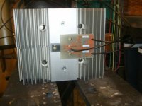
well it's a picture from my F4, but i tried it with different setup's too.
I have something else to build
Jesper.
In post #781 ( http://www.diyaudio.com/forums/showthread.php?postid=1513301#post1513301 ) I presented a compact PCB layout for F5 with Q3 and Q4 placed very close to each other. Here is a new version (bottom view, 2 x 10 cm) with Q3 and Q4 placed far apart to allow easier use of two heatsinks per channel. Parts nomenclature is the same as in previous version. As Mr. Pass said, circuit is simple enough for p2p approach but PCB makes bias/DC offset adjustments easier.
Attachments
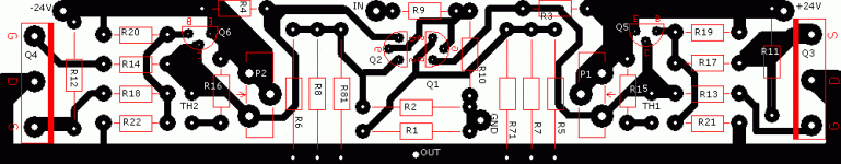
juma said:In post #781 ( http://www.diyaudio.com/forums/showthread.php?postid=1513301#post1513301 ) I presented a compact PCB layout for F5 with Q3 and Q4 placed very close to each other. Here is a new version (bottom view, 2 x 10 cm) with Q3 and Q4 placed far apart to allow easier use of two heatsinks per channel. Parts nomenclature is the same as in previous version. As Mr. Pass said, circuit is simple enough for p2p approach but PCB makes bias/DC offset adjustments easier.
Very nice , can I have a pair of them ?
stefanobilliani said:
Very nice , can I have a pair of them ?
Sorry Stefano, I don't have the means to produce and distribute PCBs but you are free to use the layout any way you like.
- Home
- Amplifiers
- Pass Labs
- F5 power amplifier