")
Goffe said:I made some changes, the J-fets are together and the feedback resistors closer. Dimension 10x3.8cm
Any advice please?
/Goffe
I Would suggest you move R13 throu R17 much coser to the power transistor, idem on the other side. It can be done very easy.
This is because R13 should be as close as posible to the Gate pin to avoid oscilations.
Otherwise the layout looks pretty good even though I din't check trace connections.
jackinnj said:Who mentioned tweaking R1/2 ? -
You can tweak the ratio of R1/R2, by a tiny amount, to improve cancellation of the 2nd harmonic. but you need a THD meter to check what you are doing is going in the right direction.
For anybody who what's to know the reason...
It is because for any amplifier circuit the the ratio of the feedback resistors only approximates the gain of the circuit because the open loop gain also has an affect too.
The equation for the actual gain is:
G = Vout/Vin = A/(1 + AxB)
Where A is the amps open loop gain.
and for a non inverting circuit B = Ri/(Rf + Ri) (or for the F5: R1 / (R5||R7+R1) or 10/(50+10)
In a normal opamp A is very high and A/(1 + A) is effectively equal to 1 so the equation simplifies to: Vout/Vin = 1/B = (Rf+Ri)/Ri
Now for the crux
In the F5 design there is effectively 2 amplifiers with 2 feedback loops and 2 corresponding open loop gains.
The first amp consist of Q1 and Q3 and the second is Q2 and Q4.
The open loop gain each amp is different which causes the closed loop gain curves to be slightly different.
If the gain curve of each half is identical then the distortions in each half is identical and then the distortions will be equal and opposite and can cancel each other out.
So if you tweak the closed loop gain of each feedback network it is possible to make the gains to be almost identical and greatly improve the 2nd harmonic distortion.
Cheers
Tim
Goffe,
I don't know much, but since Nelson said
Maybe it would be better to have the thermistor pads right next to the Output device pads so you don't need extension wires to connect the thermistors? Maybe switch the thermistor pad and related resistors with the V+or V- pads . It would be OK to have the V+/- pads more inboard I think...
Also, since the V+/- would be closer to t he center then, maybe have thin traces from the V+ and V- each come to a pad closer to a ground pad to hook up LEDs (blue of course.. - maybe on either side of the input? If you bother with the LED idea, having resistor pads next to the pads for the LED is helpful to reduce the voltage..
I don't know much, but since Nelson said
I added what is in parentases.my preference is to just glue them (The Thermisters) to the top of the plastic (The Output Devices)
Maybe it would be better to have the thermistor pads right next to the Output device pads so you don't need extension wires to connect the thermistors? Maybe switch the thermistor pad and related resistors with the V+or V- pads . It would be OK to have the V+/- pads more inboard I think...
Also, since the V+/- would be closer to t he center then, maybe have thin traces from the V+ and V- each come to a pad closer to a ground pad to hook up LEDs (blue of course.. - maybe on either side of the input? If you bother with the LED idea, having resistor pads next to the pads for the LED is helpful to reduce the voltage..
so your method is to tape on printout for drilling holes (got to find real tiny bits, hmmm)
I have used muriatic and hydrogen peroxide to etch--it works very well.
Tom Gootee had a detailed description on his website how to do it.
The really neat part of his process is using a printout of your circuit (on laserjet photopaper) as an iron-on. (apparently laser jet toner is mostly plastic). You get a really proffessional looking circuit board.
JJ
jupiterjune said:
The really neat part of his process is using a printout of your circuit (on laserjet photopaper) as an iron-on. (apparently laser jet toner is mostly plastic). You get a really proffessional looking circuit board.
JJ
I have tried this method. I also read that photopaper should be used, but it must have been another type. Got good results with standard 80g laser/copier paper.
After etching I ironed on a silk screen.
Johnny
http://www.diyaudio.com/forums/showthread.php?postid=1494067#post1494067
From earlier in this thread. My first toner transfer PCB. Easy and quite serviceable.
7/10
From earlier in this thread. My first toner transfer PCB. Easy and quite serviceable.
7/10
> So if you tweak the closed loop gain of each feedback network it is possible to make the gains to be almost identical and greatly improve the 2nd harmonic distortion.
Or you can also measure the transcoductances of the 4 transistors beforehand, and make sure (by design) that the open loop gains of both halves are identical. This is what I do.
Patrick
Or you can also measure the transcoductances of the 4 transistors beforehand, and make sure (by design) that the open loop gains of both halves are identical. This is what I do.
Patrick
EUVL said:> So if you tweak the closed loop gain of each feedback network it is possible to make the gains to be almost identical and greatly improve the 2nd harmonic distortion.
Or you can also measure the transcoductances of the 4 transistors beforehand, and make sure (by design) that the open loop gains of both halves are identical. This is what I do.
Patrick
That is true if you are using the closely matched 2SK1530 and 2SJ201 but it would be unlikely if you used the IRF240 and IRF9240.
The good thing about this complementary feedback topology is you can get low distortion without matched parts and then you can tweak it to do better.
Cheers
Tim
jacco vermeulen said:Who cares.
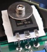
Metric : M3
UTS : 6-32
If you use the Fairchild devices a 6-32 screw is too big for the hole. I had to drill mine out (with no ill effects to the MOSFET).
re; pcb
Goffe,
I see you have been busy with the changes and thinned up the pcb - assume those measurements say 3.9" x 1.5" which makes the fet mounting holes about 6" apart - to suit long heatsink - could easily move them around to the long side to suit shorter sink.
Variac suggested the moving the th1,2 closer to the power fet which seems a good idea and the pads plus resistor for that nice blue led is easily done.
Now, if you exchanged the positions of R19 with R21 (20 - 22), could then run the fat O/P track under R17 (14) and goirectly to the fet pad - saves going around the corner - bit simpler
If you were to move the H1 (2) closer to the o/p fets, suggest moving the R3 and R15 (TH2, R4, R16) with it and so can move the V+,V- towards "front" of pcb, use some resistors as per Variac for track-jumpers for the led pads (connector?)
Hope this is of assistance ... J
Re: re; pcb
You actually need a lower impedance ground path. R1 and R2 (10 ohms) pass a bit of current through R5..8 which are in parallel with the load (assume 8R).
It's always important to have the distance from the gate stopper to gate as short as possible.
I wouldn't get so hung up about having the JFET's as symmetrical as Goffe has shown. It will make things a bit simpler if the JFETs and Zetex devices are in a "kind of X' format.
When I get back from NYC this afternoon I am going to try various values for the JFET gate stopper. I think that the 1K may be a bit high.
jameshillj said:Goffe,
I see you have been busy with the changes and thinned up the pcb - assume those measurements say 3.9" x 1.5" which makes the fet mounting holes about 6" apart - to suit long heatsink - could easily move them around to the long side to suit shorter sink.
Variac suggested the moving the th1,2 closer to the power fet which seems a good idea and the pads plus resistor for that nice blue led is easily done.
Now, if you exchanged the positions of R19 with R21 (20 - 22), could then run the fat O/P track under R17 (14) and goirectly to the fet pad - saves going around the corner - bit simpler
If you were to move the H1 (2) closer to the o/p fets, suggest moving the R3 and R15 (TH2, R4, R16) with it and so can move the V+,V- towards "front" of pcb, use some resistors as per Variac for track-jumpers for the led pads (connector?)
Hope this is of assistance ... J
You actually need a lower impedance ground path. R1 and R2 (10 ohms) pass a bit of current through R5..8 which are in parallel with the load (assume 8R).
It's always important to have the distance from the gate stopper to gate as short as possible.
I wouldn't get so hung up about having the JFET's as symmetrical as Goffe has shown. It will make things a bit simpler if the JFETs and Zetex devices are in a "kind of X' format.
When I get back from NYC this afternoon I am going to try various values for the JFET gate stopper. I think that the 1K may be a bit high.
- Home
- Amplifiers
- Pass Labs
- F5 power amplifier