Nelson stated any point from ground to source pin.
But one needs a distortion analyser to tweak this i suppose.
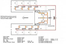
Now you remind, I remember Nelson suggested that
Could it look something like this
btw, some show a zener diode instead of resistor, I dont know why?
A word of caution
The Renesas have reversed Drain/Source over the IR devices, thus the Renesas doesnt fit into the F5 boards from PeterDaniel and Cviller
Its written on my layout to avoid confusion
Hope I got this right
Attachments
Last edited:
Hello Folks, I'd like to build an F5, can someone give me an approx. cost for a total build including cabinet, heat sinks, boards, etc.. Also, what are the critical parts such as resistors to get the best sound. Thanks in advance.
Phill
Transformers and heatsinks are the most expensive parts. (and sometimes PSU caps). The two first do not suffer from being second hand.
On big heatsinks, it is easy to screw four aluminium plates to build a cabinet.
Last edited:
Thanh
I would like to ask some question before I go on and each my PC boards .
If I understood well you drive 3 pair mosfet with 1 pair JET with out cascode .
What type of power mosfet U use ?
Do the JET can drive well the 3 pair mosfet ?
Also what is the power supply voltage of your amp ?
I ask all these because I can still modify my layout to cascode the JET in case there is a need for .
What is your opinion on that if I parallel the JETs ? I sow it in a another amp or cascode it would be better solution .
In case if I have any difficulties to drive with one pair JET the 3 pair Toshiba 2SK1529 /2SJ200 .
Would you be so kind to share your opinion . I ask all these because you wrote if you would start now your project you would go with 2 pair power mosfet only!!!?????
Better to ask now than later sorry .
You know I have the high power 2x18VAC transformer , I have the large heat sink , I want to bring out the best of these amp but also I want to use 3 pair power mosfet / channel .
Thank you very much !
Greets
1. 3 Pairs is correct
2. IRFP240 and IRFP9240
3. Yes the Jfets drive 3 pairs without any problems
4. At the moment I am using +/- 24V rails
Ok this is what I think.
From memory, I think you said you had a 1.5 kVA transformer laying around, as well as some massive heatsinks. You also mentioned you had Toshiba mosfets.
Those Toshiba mosfets have almost half the input capacitance (700pF) of the IR devices, so you are not going to have problems running 3 pairs.
I would design your board to include every feature possible, however that does not mean you have to use all the different variations, you can use links to bypass any of the options you don't use.
The reason I said I would go with 2 pairs if I was starting from scratch is that it is cheaper, also 2 pairs can be used for 3A bias (1.5A each), you don't really need 3 pairs, but if you already have the mosfets laying around and have huge heatsinks and a monster transformer then why not.
I would start with the standard version first, then go with the F5X.
I am a little worried it could be quite tricky trying to get the DC offset and bias right with 4 trim pots. Sometimes too much adjustment can get you into trouble.
With the cascode. I would allow 2 holes at one end of the resistor. One hole has a track directly to ground, the other hole has a track directly to the source pin of the Jfet, that way you can quickly test both ways if you want to try cascoding.
If you didn't already have that transformer I would probably build a 40V version with around 2A to 3A bias.
Last edited:
Thanks Thanh
Very kind from you !
I already has the transformer , because only 18VAC and yes 1.5KVA with these better to try the X .
I have another transformer 30-0-30VAC 1KVA but that only it would be OK for SE version and it will be not strong enough to bias both channel around 3A .
Also with the higher voltage need to cascode the JETs , I'm not after that much the cascode mode even do I just look up some of your simulator tests and really nice . But to many variation to cascode , to find out how it sound better .
Resistor to ground , to source , or Zener diode plus the right value capacitor ..A lot of headache!
The reason I wrote I wanted to be sure the JET will drive 3 pair Toshiba .
In case if I can not set up the right bias & offset in X mode it is still possible go bridged mode . I want to use the amp in balanced mode .
Of course how Patrick wrote and also you advised I set up first the regular F5 (each PC board) to have some experience with the bias & offset after will try to X-ed .
I have to tell you I was a bit afraid from my Aleph X to set up because I read a lot of complain etc. about but on the end it was easy .
Also the lower voltage would be better I have some large Mallory caps 400 000uF but just 30V .With some smaller caps that will be great power supply ! It was tested in the Aleph X , great caps !
I will take the risk and order the rest of the parts and I populate 4 PC board .
Thanks one more time .
Greets
Last edited:
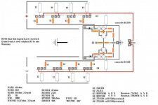
Now you remind, I remember Nelson suggested that
Could it look something like this
btw, some show a zener diode instead of resistor, I dont know why?
A word of caution
The Renesas have reversed Drain/Source over the IR devices, thus the Renesas doesnt fit into the F5 boards from PeterDaniel and Cviller
Its written on my layout to avoid confusion
Hope I got this right
Tinitus
I would like to warn you about the Toshiba mosfet the pin out is the same as the IR devices .
Please check the data .
Probably someone use your drawing for layout and will end up with a bad PC board or can blow up the power mosfets if he use Toshiba devices .
Greets
To be sure I'm 100% right I checked again .And yes the Toshiba devices pin out not the same as the Renesans !
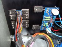
Please take a look at Smyslow populated (working) PC board .
He use Cviller PC board with Toshiba mosfet .
If U use Toshiba MOSFETs make sure your drawing is OK . I just read you wrote on your attachment the drawing for Renesans & Toshiba devices .
Please do not take it as a criticism !
Greets
Please take a look at Smyslow populated (working) PC board .
He use Cviller PC board with Toshiba mosfet .
If U use Toshiba MOSFETs make sure your drawing is OK . I just read you wrote on your attachment the drawing for Renesans & Toshiba devices .
Please do not take it as a criticism !
Greets
Last edited:
To be sure I'm 100% right I checked again .
I just read you wrote on your attachment the drawing for Renesans & Toshiba devices .
Ok
If you read my previous post again you will see that I clearly referred to Renesas only, and didnt mention Toshiba at all
Apart from that, pinout on J162/K1058 is exactly the same whether they are Toshiba or Renesas
So nothing wrong in mentioning Toshiba
And I believe they are only available in the form of Renesas devices
Renesas are often referred to as Renesas/Toshiba, but to be 100% safe I have removed any mention of Toshiba
Please also note that theres no component identification on my "board-layout"
Its intentional, because its not verified to work, yet
Attachments
Last edited:
OK you right !
I read still on your previous attachment Renesans/Toshibas
But I don't care , I check the data .
You wrong about the Renesans , they only produce the ex Hitachi devices .
Please look up the data .
Any way I do not want to argue over these .Not my cup of tea .
I'd rather make friends and learn from them ! That is more important .
The second attachment is OK , I just mentioned because some people does not read well English . Probably they see RENESANS /TOSHIBA and can make a mistake .
Please do not take it as I want to criticize you , not at all!!! Seriously.
Please take a look at cvillier board with the Toshiba mosfet.
Greets
Attachments
Last edited:
OK you right !
I read still on your previous attachment Renesans/Toshibas
Probably they see RENESANS /TOSHIBA and can make a mistake .
Ok, I really messed it up
But I clearly write 2SJ162/2SK1058
But you are right
I dont know why I thought Renesas was made on a Toshiba patent, which clearly is a Hitachi patent, and stands in BIG letters
How I could be so confused I dont know, sorry about that
Which means I should proably not be doing stuff like this
Thanks for the correction
Last edited:
The big confusion
It has been mentioned that Toshiba devices should be easier to drive
Its also been mentioned that it really mostly concerns the laterals
Its been stated that Toshibas are just another vertical
I dont know if there are any lateral Toshiba
I bought the Renesas/Hitachi laterals based on that information
Completely my own doing, as info has been rather thin and random
Facts are
Curve tracer matched quads, and Vgs with 3digit accuracy
2x quad 2SJ162 are all within 0.50 Vgs, and 2x quad 2SK1058 all within 0.83 Vgs
Seems pretty good to me
But now Im whispered in my ear that Renesas are harder to drive
Im confused more than ever
I have to deal with this somehow
But if any attempt to clarify this issue only starts another big confusion, please dont, just ignore
Last edited:
The sound I heard when unplugging the DAC sounded like an oschillating sond that got higher and higher until it dissapeared.If it involved any uhearable sound that had to be messaured to see I dont know,maybe sommeone ellse can expaine better,just hoping that none of the transistors was blown..Hi,
Can someone tell me what parasitic oscillations sound like? Is it something obvious or more subtle that needs to be measured on an oscilloscope?
Yeah, I suppose the best we can do learn from our own mistakes, and others
Unfortunately mostly we dont, and just repeat the mistakes, because thats what we do
Anyway, I have learned to trust my intuition
But man, it feels much like windsurfing in stormy weather, never knowing when you end in the water fighting fore your life
And yeah, I have been there too
Pure adrenaline rush
Somehow I think I have managed to find the balance
Quad Renesas laterals
Only 7A, thus keeping the original rail voltage
Raised bias
Cascoded Jfet
Mono with double HUGE heatsinks
It have to work, but maybe only that way
Thanks
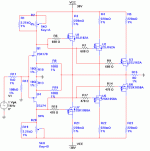
btw, where did this schematic come from
Is it just a theoretical marriage of F5 and GrandProfet
Or is it a tested proven one, or simulated, or
The difference on gate resistor, 680R on J162 and 470R on K1058, indicates something have been considered
Hmm, yeah, my J162 do have lower Vgs than K1058, is that it
And higher value of gate ressitor relates to its low Vgs, and ease of drive
But IR device seems to have lower on-resistance, I dont get it with these Vgs/Vds figures
Man, I have learned to say "gate-resistor"
Attachments
Last edited:

- Home
- Amplifiers
- Pass Labs
- F5 power amplifier