Please be aware that Vds-Id measurement should be done at constant temperature. The curve is temperature dependent.
The equipment I use employs sub-millisecond pulses. There is no temperature rise since the effective duty cycle is close to zero. The tradeoff is that the precision of the measurement is not as good as using a wide open aperture of 1 NPLC or 16.67 milliseconds.
When I start to try to match transistors, I may slow down the measurement and have the transistor on a heatsink.
The curve above that ends around 10A required no heatsink.
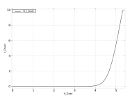
The family of curves is very uninteresting for this transistor since 99% of the usual stuff you see in these curves is well beyond any measurement rig except for one very expensive rig.
That is why I traced the Vgs - Id curve. I can see pretty much all I want to know with this curve and not have to go beyond 10A.
Matching and temperature dependency measurement will be needed once parallel output stage is utilized.
Understood. We will get there.
I am thinking of wiring up the OPS and seeing how just the output behaves.
Here is an additional piece of information.
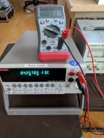
RDSon of the N-FET is about 4.1 milli-ohms.
Test conditions
Vgs = 10V applied
Ids = 1.0A applied
Vds measured = 4.06 millivolts
This measurement includes all of the FET drain and source lead lengths and a few millimeters of copper wire soldered to the FET to mount the FET in a banana plug with drain and source fastened into the banana plug. The banana plug was inserted into a DMM to take the Vds voltage measurement.
This measurement would be easily repeated by others using a DMM, two channels of power supply and one power resistor to set 1A through drain and source.
I happen to have an accurate current source, accurate voltage source and a good benchtop DMM.
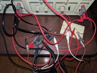
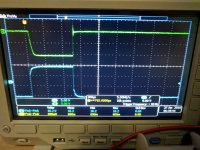
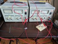
Here is the OPS rats nest. The bias is simply two resistors and two pots. Two adjustable power supplies are used.
The output load is a 1k resistor.
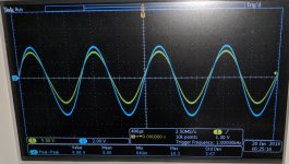
Power supplies were operated between +/- 5v to +/- 6V. In the scope shot, yellow is the input and blue is the output.
Messing with the pots and the power supplies, I did get the offset close to zero eventually.
Time to mount the outputs on heat sinks and break out some perf board.
cheers
The output load is a 1k resistor.
Power supplies were operated between +/- 5v to +/- 6V. In the scope shot, yellow is the input and blue is the output.
Messing with the pots and the power supplies, I did get the offset close to zero eventually.
Time to mount the outputs on heat sinks and break out some perf board.
cheers
Attachments
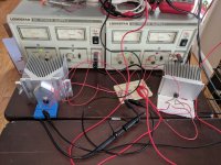
Attached are pictures of the OPS mounted to heat sinks to allow some bias current to flow.
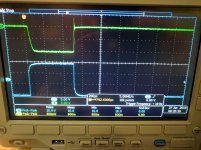
These FETs do not like to be at + - 5V with the bias resistors on the same +/-5V. The Vgs_on of the NFET is 3.8-ish and that places the gate too near Vcc to have any meaningful voltage swing.
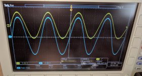
I changed the rails to +/- 8V and that allows the NFET to produce some output.
The sig gen craps out at 20V p-p so I cannot drive the output stage to clipping.
Looks good enough to build the rest of the amp and get it all running together.
These FETs do not like to be at + - 5V with the bias resistors on the same +/-5V. The Vgs_on of the NFET is 3.8-ish and that places the gate too near Vcc to have any meaningful voltage swing.
I changed the rails to +/- 8V and that allows the NFET to produce some output.
The sig gen craps out at 20V p-p so I cannot drive the output stage to clipping.
Looks good enough to build the rest of the amp and get it all running together.
Attachments
put bias network on higher rails , leave drains at lower
install diode clamps between drive node and output
Post #1146 has the schematic showing higher voltage for input through Vas. The output FETs are the only thing on the lower voltage rails.
Thanks for the tip about the diode clamps.
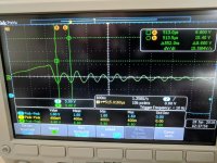
Here is the N-channel FET in a test of high current. The FET is simply used in class B mode. The gate is driven by a 15V pulse. The blue trace is the 15V, 500 uS gate pulse. The green trace is the voltage across a 0.1 ohm resistor that is connected from the FET source to the power supply negative. I measured from the Fet source to power supply negative because I lack a differential probe to lmeasure the voltage across a resistor from drain to power supply positive.
So, a tiny bit more than 100A flowing through the FET.
I want to call this amp "The beast with a hundred amps (Amperes)". Has this name already been trademarked here?
Next I will start to characterize all of the output FETs and look for the closest match for transconductance curves, etc.
The building of a channel will commence soon.
Attachments
Well done Woofertester this is the kind of stuff I like to see real world measurements.
I'm surprised at the delay in the rising edge of the input pulse and the slope not as fast as I thought it would be. Secondly the overshoot and ringing at the end is this due to the power supply recovering?
I'm surprised at the delay in the rising edge of the input pulse and the slope not as fast as I thought it would be. Secondly the overshoot and ringing at the end is this due to the power supply recovering?
Well done Woofertester this is the kind of stuff I like to see real world measurements.
I'm surprised at the delay in the rising edge of the input pulse and the slope not as fast as I thought it would be. Secondly the overshoot and ringing at the end is this due to the power supply recovering?
I believe the delay of the rising edge is because the FET is not biased. The 15V pulse must rise above Vgs_on (4.5-ish volts) before the FET turns on.
The ringing at the end of the pulse is, I believe, a device phenomena. The cure may be a series RC zobel across gate and drain.
9.2v pk across 0.05 ohms, 184 Amperes. The datasheet for the N-channel part states that 200A is the max that can go through the package wiring. So we stop here looking for more current.
Next is the ringing upon turn off. The frequency of oscillation is about 1.8 MHz. I will try various gate stop resistances and RC snubbers across the drain and source.
Next is the ringing upon turn off. The frequency of oscillation is about 1.8 MHz. I will try various gate stop resistances and RC snubbers across the drain and source.
Attachments
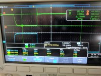
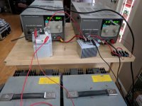
The bias circuit is powered by + / - 24V. The bias circuit is two resistors of 3.3k ohms each and and two 1k ohm pots.
The intent is for the entire front end to run at + / - 24V.
The next step is to see if the OPS can pass a sine wave, square, triangle.
The intent is for the entire front end to run at + / - 24V.
The next step is to see if the OPS can pass a sine wave, square, triangle.
Attachments
Last edited:
- Home
- Amplifiers
- Pass Labs
- F4 Beast Builders