Why only the so famous P3A is so layout dependent?
Or am I missing something....
All amplifiers are layout dependent. The layout is as important as the design. Poor layout will induce noise/distortion and in extreme cases can cause oscillation. CFPs are a little more critical than most other designs. They like to self destruct if everything isn't perfect.
Many thanks.
I understand the need of a thermal contact between Q9 (vbe multiplier) and a driver.
I spent last 3 hours making a new layout, i will post it right now.
I elaborate it from the public schematics of P3A on Elliot site. Got to do minor adjustements regulating the grid of the software in order to place the components with mmetric precision.
I hope someone will look it in detail and suggest some adjustment.
regards
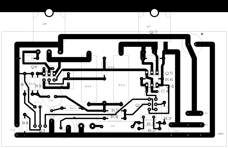
It's a little tough to follow without a schematic, but it looks like your input transistors are right beside your power rails. Power rails and output (including emitter resistors) should be in one area and the sensitive input section as far away from them as possible. Traces should be kept as short as possible, especially anything to do with the input section.
The driver transistors should be placed closely together. Place them and Q9 on a single small heat sink so they are all the same temperature, otherwise your bias will be unstable.
It's also good to look at the big picture when doing a layout. Figure out how this would mount in a chassis. The layout should allow for the input section of the amp to be mounted as far away as possible from power supplies, with as little input wire length as possible. Chassis layout should allow for the shortest power wiring as possible. All parts of the whole amplifier only add noise to the amplifier, so they all need to be considered from the start for best success.
Last edited:
ok, many thanks.
but, in the previous layout I posted (the blue one) Q5, Q6 (driver) and Q9 (vbe) are on the same line just to put them on a little heatsink so they can have the same temperature...
I don't know what doesn't go in that layout...it seems also that the input area is separate enough from the power rail and the outpu rail...
the second layout I posted is the same as Mr. Elliot PCB, the components are placed exactly the same way...probably Mr. Elliot pcb is a little smaller and all the components are nearer but it changes 1-2cm at all, I think.
So, what to do at the end?
I would buy the pcb from Mr. Elliot, but shipping cost and timing drom Australia to Italy are very L-O-N-G, as himself says on his webshop...
What can I do?
All amplifiers are layout dependent. The layout is as important as the design. Poor layout will induce noise/distortion and in extreme cases can cause oscillation. CFPs are a little more critical than most other designs. They like to self destruct if everything isn't perfect.
Sure, I know. I mean P3A is excessibly addictted to layout. Or at least is the only one that people use to quarrel about.
Member
Joined 2009
Paid Member
CFPs are a little more critical than most other designs. They like to self destruct if everything isn't perfect.
It's not that bad - true that they are susceptible to oscillations but we have close-by rail decoupling and a base-collector capacitor on the output device closest to the negative rail. For extra precaution a similar capacitor could be added to the layout for the other output device but not fitted unless needed.
I suspect those outputs that have blown up did so because of cross-conduction which CFP can suffer from. But this is usually at frequencies above the music so you probably need both an oscillation problem and cross-conduction. I found that one cure for cross-conduction is to have plenty of current through the drivers. I think Rod has nailed the design parameters so this shouldn't be a worry.
I think you may be correct with the cross conduction. If I recall correctly, Vzaichenko's CFA-CFPx2 amp blew the outputs when he tried using MJL21193/21194 due to cross conduction. He replaced them with faster IRFP240/9240 Hexfets that he happened to have in stock at the time and the problem was solved. It turned out to be a great amp in that form.
ok, many thanks.
but, in the previous layout I posted (the blue one) Q5, Q6 (driver) and Q9 (vbe) are on the same line just to put them on a little heatsink so they can have the same temperature...
I don't know what doesn't go in that layout...it seems also that the input area is separate enough from the power rail and the outpu rail...
the second layout I posted is the same as Mr. Elliot PCB, the components are placed exactly the same way...probably Mr. Elliot pcb is a little smaller and all the components are nearer but it changes 1-2cm at all, I think.
So, what to do at the end?
I would buy the pcb from Mr. Elliot, but shipping cost and timing drom Australia to Italy are very L-O-N-G, as himself says on his webshop...
What can I do?
Somewhere on this forum I have seen a pcb designed by alex mm
I have built this and I think it's one of the best that have been presented for this amplifier.
I will try to find if there is any interest.https://www.youtube.com/watch?v=LUgWjOxNueo
Last edited:
Somewhere on this forum I have seen a pcb designed by alex mm
I have built this and I think it's one of the best that have been presented for this amplifier.
I will try to find if there is any interest.
Thank you, it will be great!!!
http://www.diyaudio.com/forums/solid-state/164756-p3a-comparison-table-long-31.htmlThank you, it will be great!!!
Reed some pages and see details.
Member
Joined 2009
Paid Member
I think you may be correct with the cross conduction. If I recall correctly, Vzaichenko's CFA-CFPx2 amp blew the outputs when he tried using MJL21193/21194 due to cross conduction. He replaced them with faster IRFP240/9240 Hexfets that he happened to have in stock at the time and the problem was solved. It turned out to be a great amp in that form.
I did have some problems with my CFP output (search up for the TGM8 amplifier) but solved them in the end. I don't think there's so much of a worry with P3a, it's a simpler design and well-proven. However, as we like to chit chat about all our experiences it can create the perception that this design is somehow difficult to work with - it's not, it's a great design even for beginners to play with and some well meaning folk on this forum to help out if there's a problem.
I hope you don't give up on your layout, it looks like a good start to me, there is a nice feeling from seeing the results of your own work. And pcb's are cheap from China so you can afford to re-spin the design if you need.ok, i wait for your opinion about a valid layout for this amp
Last edited:
I wonder why somebody would even consider making the Chinese rich while Rodd Elliott is offering the proper PCBs for this project, as many as you want, NOW.
To boot, quite inexpensive.
And he *deserves* getting a couple dollars back, if any to help pay his server costs.
In theory DIY audio is against ripping Commercial products ... and then not even winks about profiting from a generous contributor?
I don´t get it.
To boot, quite inexpensive.
And he *deserves* getting a couple dollars back, if any to help pay his server costs.
In theory DIY audio is against ripping Commercial products ... and then not even winks about profiting from a generous contributor?
I don´t get it.
I wonder why somebody would even consider making the Chinese rich while Rodd Elliott is offering the proper PCBs for this project, as many as you want, NOW.
To boot, quite inexpensive.
And he *deserves* getting a couple dollars back, if any to help pay his server costs.
In theory DIY audio is against ripping Commercial products ... and then not even winks about profiting from a generous contributor?
I don´t get it.
Cucicu has already mentioned that Rod Elliot's website states there are issues when he ships to Italy. I believe he plans to hand etch boards.
I wonder why somebody would even consider making the Chinese rich while Rodd Elliott is offering the proper PCBs for this project, as many as you want, NOW.
To boot, quite inexpensive.
And he *deserves* getting a couple dollars back, if any to help pay his server costs.
In theory DIY audio is against ripping Commercial products ... and then not even winks about profiting from a generous contributor?
I don´t get it.
Mr elliot p3a is a pubblic project, so everyone can play it as he like.
Ah, there are about a hundred of posts anout p3a layout on this forum
Hey men
I make a good layout. Thanke to my greek Friend; )
Do you think it's a good idea to make just one pcb for channel, each one with supply caps (2×10.000uf), amp and speaker protection?
Everyone has their own theories for layout, but you are likely better to leave the 10000uF caps at the supply, and return your speaker grounds there. That little extra distance can help with noise on the supply.
You forgot to show some pictures.

Everyone has their own theories for layout, but you are likely better to leave the 10000uF caps at the supply, and return your speaker grounds there. That little extra distance can help with noise on the supply.
You forgot to show some pictures.
Ok...probably is better this way...
Do you think is better to make a pcb with supply cap (snap in) ore use cap woth screws (not pcb) and cables?
Ps pictures will come tomorrow as I will print the boards
Either way is fine for the supply. I usually use boards with snap ins just because it's a little neater to mount.
It would be nice to find a schematic with all the link from trafo to diode brdge to caps to amp and the masses
- Status
- This old topic is closed. If you want to reopen this topic, contact a moderator using the "Report Post" button.
- Home
- Amplifiers
- Solid State
- ESP P3A Layout