Hi superR - I'm a little late to your amp build party and what a party it is turning out to be! After having read through some of this thread now, I feel your pain. Trying to discover the 'correct' method here can be a daunting task. There are a lot of experts here, yet many will offer contradictory suggestions. Proceed with caution is the monicker I've adopted. It can be quite a jungle in here - if you know what I mean. 😀Well if the guys who give advice need advice too, I might need a book on class ab layouts, can any of you advice some literature?
I'm not into doing my own PCB layout, so your way ahead of me there. 🙂 I just opted to purchase ready made amp modules myself, but I would not recommend that path for others whom want to really understand and tweak their own designs. You could just buy well-known, reliable blank PCBs and go from there too with your own components. That way you can still customize it with the grade, quality and tolerance of each part. Good luck.
You just summed up about 50% of the questions on the Solid-state/PCB-ing department. Fortunately I ended up with a nice result which does not only work well but seems to measure nicely on THD+N. The comment that really boosted performance was that of adding a 10R resistor between powergnd and signalgnd. That impact could be measured in the low frequency regions.
The fact that I did not order a prefab PCB was that none suit my wishes on dimensions or the use of connectors.
The fact that I did not order a prefab PCB was that none suit my wishes on dimensions or the use of connectors.
I congratulate you on a job well done. Your perseverance paid off. I love to build things and find these type projects challenging to get the right sound and look I demand. I'd say you achieved both! 🙂 
Redjr,I congratulate you on a job well done. Your perseverance paid off. I love to build things and find these type projects challenging to get the right sound and look I demand. I'd say you achieved both! 🙂
I think SuperR can vouch for the fact that you cannot plan what a PCB will do. What you can do is to avoid some obvious pitfalls which are mostly logical anyway and one learn by mistakes.
I must also say that there is a lot of pride and enjoyment to be had from making everything from scratch, I think SuperR can tell you this also.
Like I always tell to my friends; I am no electronics guy. I just like to built things. This time it's an amplifier, maybe next week I'll be upgrading the kitchen furnace. 🙂
The thing I am most fond of, is the fact that yesterday morning the amp was a pile of parts which worked separately, one and a halve day later it looks like an amplifier without hitting major bumbs on the way.
On to the next project!! Maybe put my sub-amp in a double-enclosure....... Who knows.
The thing I am most fond of, is the fact that yesterday morning the amp was a pile of parts which worked separately, one and a halve day later it looks like an amplifier without hitting major bumbs on the way.
On to the next project!! Maybe put my sub-amp in a double-enclosure....... Who knows.
The amp is a 90% copy of Elliots P3A and the pcb layout and schematic adjustments have been made by me in order to make the pcb fit vertically in the 80mm high enclosure.
Hi!
Would you mind posting your pcb artwork? I just wanted to have a look at it. I also built a proto of the P3A using Jlester's lay-out only that I did a few mods of my own. The amp sounded clean no distortions whatsoever..🙂 I'm just not quite content on the DC-offset reading, I get 27mv. Here are the parts I have used..
p-output = 2SC5200/2SA1943
drivers = MJE15031/15032
vas = 2SA1209
input pair = MPSA42
Regards!

Last edited:
In the revised p3a the output transistor emitter resistors were increased along the lines put forth by Leach, in which he shows that the output gm is practically constant for all output currents, with a particular Re and Ib.
The expression he gives is Re = Vt/Ib
Since Vt is temperature dependent, stabilising Ib by thermal feedback results in the gm varying with temperature unless more bias current is used in the first place, so letting Ib rise with temperature keeps the bias current in the optimal range withought excessive quiescent current and this works perfectly well if an adequate heatsink is used.
rcw
Hi!
I am not so familiar with "figures" (I'm still working on it😉) but because I'm using 0.22 ohms emitter resistors instead of 0.33 ohms as per the revised schematic, will this mean that varying the emitter resistors greatly affects dc-offset?
Regards!
I am not so familiar with "figures" (I'm still working on it😉) but because I'm using 0.22 ohms emitter resistors instead of 0.33 ohms as per the revised schematic, will this mean that varying the emitter resistors greatly affects dc-offset?
Regards!
The input pair balance has the greatest effect on the offset.
Using smaller emitter resistors means that in your case the Ib for linear gm is 120mA. instead of the 52mA. of the revised circuit with .5 Ohm resistors.
For a 40 degree temperature rise the Ib goes up to 134mA. for .22 Ohm. and 59ma. for .5 Ohm.
You get about 1.2db. more power output for an amp that runs hotter, and has much more quiescent current.
rcw
..the input pair, yes I have noted that I actually wanted to use low noise and higher gain devices like 2N5088 or MPSA18 and see if it will make a difference.
TY!
TY!
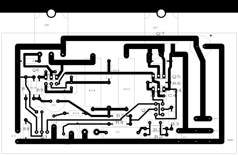
This is my current layout. Maybe with some minor changes but the basics are there. http://www.diyaudio.com/forums/solid-state/212342-esp-p3a-layout-10.html#post3043548
Instead of the BD139/BD140 I have used MJE15030/31, for the output I have used NJL21193/94 and the other transistors are BC546B. Input caps are just cheap 0.30 $ /piece items so the most luxurious item are the output transistors.
In practice DC offset is around 4 mV. The layout is not 100% to my likings, but so far it works nicely.
I'm surprised you're quite right very simple...thinner traces so similar to the original P3A board perhaps Rod was right in saying...."Note that the layout of any power amplifier is quite critical, and great pains were taken to minimize problem areas - if you make your own PCB, it is unlikely that you will be able to match the published specifications."
🙂
🙂
It's up and running for about a day or 2 so it needs some work and testing but so far it's performing quite well. I still need a proper dummy load and attenuation so I can record the output on my pc. The story isn't over yet but so far I am pleased, especially about the clean look.
My second P3A amp dc offset reading is only 3.1mv. Matching transistor in differential amplifer is very important by just using a digital multimeter with hfe tester. I'm using the 2N5551 for the diff amp and constant current source. I bought 20 pieces of 2N5551 and match its hfe. Then select the best match pair for the diff amp.
hi guys, what do you think about this P3A layout?
An externally hosted image should be here but it was not working when we last tested it.
hi guys, what do you think about this P3A layout?
An externally hosted image should be here but it was not working when we last tested it.
This layout is made by someone who thinks that he has an idea of how P3A works ...You need to do some reading to understand how many mistakes you have on this layout ...
This layout is made by someone who thinks that he has an idea of how P3A works ...You need to do some reading to understand how many mistakes you have on this layout ...
can you explain please? many thanks
Member
Joined 2009
Paid Member
Sakis has HUGE experience with this amplifier and knows how to optimize every last drop from the layout, wiring and choice of parts - but perhaps he's a bit grumpy with beginners 🙂 - it's good advice he gives to read through this thread once more and search for related threads as there is a wealth of information out there, the challenge sometimes is to sift through all this unsorted information and separate out the opinion from the facts!
I haven't looked at your layout in detail, but it looked pretty good at first glance. I'm sure Sakis can point out what we have missed ?
A couple of things:
You likely don't need to put the output drivers on the (main) same heatsink as the output devices, if you run the amplifier with all the voltages and currents as it was intended the drivers won't need a heatsink. With a CFP output you want the thermal control of the bias current to be formed from the Vbe multiplier being in contact with one of the driver devices because the driver devices themselves firmly control the operating point of the output devices. The drivers are the 'masters' and the output devices the 'slaves' in this type of output topology.
Your output connector will be easier to use if you allow more space around it.
Last edited:
Many thanks.
I understand the need of a thermal contact between Q9 (vbe multiplier) and a driver.
I spent last 3 hours making a new layout, i will post it right now.
I elaborate it from the public schematics of P3A on Elliot site. Got to do minor adjustements regulating the grid of the software in order to place the components with mmetric precision.
I hope someone will look it in detail and suggest some adjustment.
regards
- Status
- Not open for further replies.
- Home
- Amplifiers
- Solid State
- ESP P3A Layout