For low current noise OPA1642 is much better than OPA1656. Also lower 1/f voltage noise.Opa1612 has very high current noise, opa2210 has the same current noise as 5534a but less voltage noise. With low impedance source 2210 and 5534a are nearly similar knowing that my 10k input resistance dominates the voltage noise
This one : https://www.waynekirkwood.com/image...gh_Performance_Siliconix_AN81-3_July_1983.pdf ?Siliconix has an application note of 5534. Any one knows where to find?

For low impedance source, bipolar gives lower noise but if jfets are better for high impedance because lack of current noise, what is the meaning of using ultra low noise jfets. With 10k source, it has already 13nV/sqrt Hz. This why any fet transistor as 2n7000 is OK.
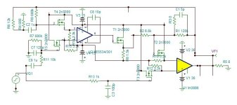
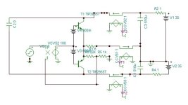
As I am using the opamp in open loop mode, the output impedance linearity gets important.
I will buffer the output of pin5 instead of pin6 with a 2n7000 and try to cancel the even harmonics by adjusting a resistor between pins 5-6 which increases the bias current of the output stage.
@AIM56, je vous remerci.
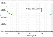
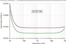
I made an LTP equivalent to NE5534 using bc550c. Then I buffered with 2n7000 the inputs.
The result is 13.8nV/Hz½ and 13nV/Hz½ with 2n7000s which is the same as total replacement with external 2n7000 LTP. I will use 2n7000 just as input buffers to get at least precise offset.
What concerns the output impedance, the above mentioned site measured about 17 ohms, probably at 100khz because the output emitter follower is driven by high impedance darlington with CCS. Simulator model gives 1k. Here the mosfet buffer can do something important.
Attachments
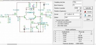
Something good comes along buffering the bipolar LTP is lower distortion. In open loop, pouring out 8mV differential, it passes from 0.0004% to 0.0001%. Of course these are very low numbers to be submitted to over 80db NFB.
If I use external LTP made of 2n7000 at 2ma bias, I get 2mV output and 0.0006% THD.
If I use external LTP made of 2n7000 at 2ma bias, I get 2mV output and 0.0006% THD.
Attachments
I also buffered the power opamp inputs. They don't act as antenna, and the phase shift at high frequencies decreased. The 10k input resistor can be decreased to 1k if volume potentiometer is not needed.
What concerns the power supply bypassing, it will excite many to see this scheme.

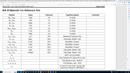
The DS says the following.

If you understand electronics, the low frequency bypass capacitor is 10uF minimum but to be 20uF if the wires supplying the DC are over a couple feet. The 470uF minimum is not on each rail but a single in between, to average the rectified current. I know this technique from single floating supply. I add just at the supply pins 100nF 100v in SMD on the bottom side.
What concerns the power supply bypassing, it will excite many to see this scheme.
The DS says the following.
If you understand electronics, the low frequency bypass capacitor is 10uF minimum but to be 20uF if the wires supplying the DC are over a couple feet. The 470uF minimum is not on each rail but a single in between, to average the rectified current. I know this technique from single floating supply. I add just at the supply pins 100nF 100v in SMD on the bottom side.
Attachments
IT is NOT one 470uf. Each rail has its own capacitors, in lm3886 case is 2X 0.1uf or more +2x10uf(or more)_+2x 470uf (or more). OF course this is for a dual rail power supply.
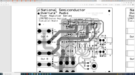
Take a look at the LM4780 (2 of lm3886 in one chip) artwork National provided in datasheet.
Take a look at the LM4780 (2 of lm3886 in one chip) artwork National provided in datasheet.
Attachments
Last edited:
So, you have 2x470uF or more on each rail, hey wait a minute, to avoid low frequency sagging resulting motorboating, you need 10uF in parallel. But, if you have long supply wires over 2 feet, you need to parallel the 470uF minimum with 20uF or more.
On would say a literature extract from "Alice in wonderland".
It is clearly said: to avoid rectified current of the load to enter back into circuitry......it should be right at the package terminals.
Only a single capacitor across the rails can comply such function.
On would say a literature extract from "Alice in wonderland".
It is clearly said: to avoid rectified current of the load to enter back into circuitry......it should be right at the package terminals.
Only a single capacitor across the rails can comply such function.
I modeled an output stage with standard 510uF supply bypassing and with 470uF between rails and 10uF supply bypassed.
The currents of the output and the rails are measured.
Standard.

With intermediate capacitor

The electromagnetic radiation of the standard is highly harmful.
The current through the intermediate capacitor is of course full wave.
As on circuit, on PCB too the intermediate capacitor must not share traces with the supply bypassing. The problem is how to put it nearest possible such a big capacitor 15x25mm the smallest or 18x30 for 1000uF.
The currents of the output and the rails are measured.
Standard.
With intermediate capacitor
The electromagnetic radiation of the standard is highly harmful.
The current through the intermediate capacitor is of course full wave.
As on circuit, on PCB too the intermediate capacitor must not share traces with the supply bypassing. The problem is how to put it nearest possible such a big capacitor 15x25mm the smallest or 18x30 for 1000uF.
Attachments
Last edited:
- Home
- Amplifiers
- Chip Amps
- Error Corrected Chip Amplifiers, aka Modulus Clone