@chromenuts lovely build, I'm tempted to try Bisesiks transformers with my D3 too. It looks like you aren't using an output buffer?
No output buffer.
I hadn’t come across any information that mentioned it was required or recommended in this scenario…although I thought I came across something in a thread discussing a tube iv solution?
Of course I’m accomplishing these projects by riding on the coat-tails of those who have the real ability to understand/design these projects and share their wealth of knowledge in a way that I can barely understand if I’m lucky. 😉
I read as much as I can and ask a lot of questions.
I’m kind of painting by numbers here…if you know what I mean?

@chromenuts fantastic build, well done! I am collecting all the parts to build my first D3 DAC, all great fun and enjoyable
I actually have a bunch of D3 related components left over.
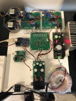
D3 built and tested by Ryan, (2) original I2S to simultaneous boards as well as the CapMX and a transformer & misc.
Most came as a bundle deal when I bought the transformers in the swap meet.
I had considered going the same route as Ryan with four D3 boards run balanced, but the complexity and having to start over with a case that could accommodate the setup put me off.
Instead I’m thinking of a second DAC build using a single D3 board for my other system.
I’d have to come up with another input/interface to I2S solution…maybe something with USB this time.
Open to suggestions.
I was able to find it.
It reads like an amazing piece of kit. Price to play is 240 Euro though…ouch!
I’m not sure it’s really my speed.
I’m honestly happy playing Redbook from my collection of a couple hundred CDs on my DIY Shigaclone transport.
If I want to hear something else I stream lossless from iTunes on my old Mac Mini with Bitperfect through Toslink to the DAC.
I don’t know that I really want to chase after all the high resolution capabilities right now.
The I2S over USB seems like it might be worth a shot.
I am starting my D3 build and I already have roadblocks. Most of mlcc are X7R on BOM, I have always used cog/npo because of the piezo-
electric effect X7R can have. I am trying to build a "pure" as possible audio signal reproduction, why would I want any ringing? Problem now is finding a cog/npo smd capacitor. Has everyone been using X7R capacitors. I have already done I2S board with X7R capacitors but really wanted cog for D3 board. I don't see any post along this idea, but I really want the best signal quality I can get. Crazy or not? I guess I just want to hear everyone is happy with X7R caps in system.
regards,
Steve
So I am having a hard time getting my head around what I have wrong so seeing it in writing helps sometimes. I have 26 volts from PS board on DMM so I assume +13 to -13 vdc. At V1 adjust [1] = 4.0vdc/ output [2] = 5.0 vdc / input [1] = 6.5 vdc not +13. On CC1 adjust [1] = 19.7 vdc / output [2] = 18.6 vdc / input [3] = -8.2 vdc which is what arrives a X3. R15/R16 = 237.5ohm parrallel divides 5 vdc 2.5vdc. 237.5ohm R16 in series with R21 5K1 to -13 vdc rail and adjust [3] of CC1 measuring 19.75 vdc which outputs[2] 18.6 vdc to R22 10R back to negative rail and input [1] measures -8.2 vdc which shows up at R30 of X3. It is not a hard board to build half wave rectified 2 diodes, two transistors , 4 resistors and the caps and I have 26 Vdc. V1 input is 6.65 and CC1 adjust is 19.75 vdc = +26.4. I only get -8.2vdc to 15 vdc rail? And why from input pin? There is only 1 way sot-223 can be oriented. I need to put PS on scope I guess see if rails are right voltages. Transformer is dual 24v secondary in CT configuration which measures 24vac each leg to center. Thanks for any help. Has anyone got measurements for V1 & CC1 and input side of R30. I do get +/- 5 vdc at 1541 inputs. Thanks for any help.
best regards,
Steve
best regards,
Steve
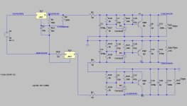
So my version is different R's numbered different with different values.R1/R2 are 15&16 2K and 270R 237.5R parallel not 290. X3 voltage divider for ref has a 10R between 1K & 3K on 3K side which is R27,28,29. My I of CC1 is -8.2 vdc to X3. My I for V1 is 6.6 but have 5.0 out. X3 ref to anode = .75. I am testing with load but 600R for X3. I have only limited parts on pcb to verify voltages to pins 15,26,28. I have tried different TL432 with same numbers resulting. I am having a hard time getting my head around CC1 with -26 to output and input to shunt reg. I don't get how this works but I am self educated and don't totally understand some of this yet. My thinking is -26 to ground [pin 14 of 1541] so to output CC1 Input to voltage divider for reference, cathode to Rs[ 100R ] to emitter of PNP, and cathode to base for regulation -15 at collector. TL431 is not cathode at pin 2 TL432 is as is the on-semi in BOM which my schematic indicates [pin 2 cathode]. So R20 on your attachment is only -8.2 vdc for me and I don't think that can get to -15 with shunt reg. but somehow I have -5 vdc on other shunt reg??? Sorry to ramble but I am hoping it helps the light come on. Can you or anyone else Let me know what input of CC1 should be. Thanks for help!!
electronically challenged,
Steve
electronically challenged,
Steve
Attachments
Steve, When I built my D3 years ago now, I had power supply problems too. What I found was that the smd TL431 was easily damaged. A easy check is to check for the presence of Vref = 2.5V. If it is not present then there is an issue with the TL431, either blown or as Ryan suggested a bad solder joint. If Vref is present then the smd transistor may be damaged or bad solder joint. My experience was that those small devices were easily damaged by too much heat.
The presence of -5V and +5V indicate that those circuits are good. The third circuit is -10V, which is in series with -5V for a total of -15v for the dac -15V.
The presence of -5V and +5V indicate that those circuits are good. The third circuit is -10V, which is in series with -5V for a total of -15v for the dac -15V.
I use an adonstar microscope so I get a pretty clear look. I will upload some images tomorrow. in the meantime I was hoping to use a twisted pear audio spdif CS8416 transceiver for I2S signal but it is a pin header for I2S. They also have a 4:1 spdif switch that has a ufl or pin input. I don't need the switch part of the board but can I use pin/ufl as in picture. Will signal be compatible with 50ohm coax of ufl?

I've been chasing my own tail! I redid my test load jig and my numbers are perfect!! My -15 pin must not have been making good contact. So thanks for your help though it is appreciated. Any info on converting a THT header to UFL. I could have a pcb made with pin via's in and ufl connector pads. Any such item out there already?
regards,
Steve
regards,
Steve
- Home
- Group Buys
- DIY TDA1541A PCB "D3"