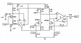
I thought I could combine Samuel Groner's Laboratory Grade Measurement Amplifier from Linear Audio Volume 3 and combine it with a design Scott showed. Much simplified here no CCS. Instead of offseting the input of U1, the potential on Q1 and Q2 should be about the same.
I have +/- 13VDC from a NiCad battery pack on an HP meter which had gone wonky over the years, and need a bit wider frequency range:
I have +/- 13VDC from a NiCad battery pack on an HP meter which had gone wonky over the years, and need a bit wider frequency range:
An externally hosted image should be here but it was not working when we last tested it.
I don't know which "original schematic"--surely mine is pretty different.
Again, the servo loop makes no sense (to me at least) as shown. It may work with perfectly matched simulation-world FETs, but try inserting a small DC voltage in series with one of the gates to simulate mismatch (then check the output voltage of U2--it should not hit a rail). If you drive R1/R10 differentially rather than common-mode this should look better.
Samuel
I've quickly sketched a concept that should be implementable: lab_grade_preamp_differential_version_r1.pdf
The fundamental disadvantage is that the input stage necessarily runs at a quiescent current close to that given by the Idss of the input JFETs. There's a plethora of disadvantages from this (e.g. WRT secondary noise sources)--at higher circuit complexity this could be adressed by providing a DC common-mode voltage to the gates which biases them negative WRT ground.
Samuel
This works quite well, I have built one for my lab. The FET's should be matched and/or you can trim offset at the drains. The gain resistor goes between the sources. The bias current of the FET's is set by the current source (J3) and U1-A servoing the voltage across the 500 Ohm resistor (I used AD823's).
Advantages, can be used DC since the commonmode feedback is active and the circuit is quite simple. The catch is the min gain does not include 1 but that is rarely necessary. Cascodes could be added but I'm not sure they are necessary.
BTW this is an abandoned concept for a real IC.
EDIT - you can play with the values if you need a larger DC common mode range, the 4K might be overkill on gain out of the FET's
Attachments
Last edited:
Scott-
I would think that the 1K source resistors would limit the noise performance. The source to source resistor, not shown, would be the dominant noise source but the 1K resistors do limit what can be done. Also wouldn't the output impedance of the opamp affect the differential gain? Maybe that is intentional?
Couldn't the biasing also be done by setting a fixed voltage for R9 that represents the target current in R7?
Scott-
I would think that the 1K source resistors would limit the noise performance. The source to source resistor, not shown, would be the dominant noise source but the 1K resistors do limit what can be done. Also wouldn't the output impedance of the opamp affect the differential gain? Maybe that is intentional?
Couldn't the biasing also be done by setting a fixed voltage for R9 that represents the target current in R7?
All in-amps have that issue, but what about any resistive feedback amp at low gain? The feedback resistors dominate at low closed-loop gain, the same would be true of the original circuit. This circuit actually does better at low gains than any commercial in-amp I know of including the THAT1510, and our own SSM2219. For mic or phono use I don't see using gains of less than 100 or so, there the gain resistor and the FET's totally dominate the noise.
On the second question I don't see your point the output impedance of the op-amp is inside the loop just like any circuit of this type. It's just a "current feedback" instrumentation amplifier with a common mode loop that gets you a single ended output with one less op-amp. The traditional version uses a 4 resistor bridge + op-amp which totally dominates the noise at low gains as here the 4 - 1k resistors do.
Scott,
When you write that this concept has been abandoned for real IC, what is the reason behind this? Is it difficult to get the same performance in an IC or are there better alternatives available when integrating the circuit?
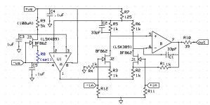
I am working on a design using the same basic concept, but with a different DC bias control. I plan to use an LSK389 with a cascode.
When you write that this concept has been abandoned for real IC, what is the reason behind this? Is it difficult to get the same performance in an IC or are there better alternatives available when integrating the circuit?
I am working on a design using the same basic concept, but with a different DC bias control. I plan to use an LSK389 with a cascode.
Scott,
When you write that this concept has been abandoned for real IC, what is the reason behind this? Is it difficult to get the same performance in an IC or are there better alternatives available when integrating the circuit?
I am working on a design using the same basic concept, but with a different DC bias control. I plan to use an LSK389 with a cascode.
The common range is too small, this is very important in a general purpose IC but in audio if you have 10V AC of common mode 50/60 Hz you have worse problems. You can fix the common mode range but that increases the minimum gain of the circuit. Again folks are used to having a minimum gain of 1 in a general purpose part.
I will post an update of values for BF862 or LSK389 this weekend. The noise is ~5.7nV refered to input at 6db of gain (the minimum no Rg), none of the IC in-amps are even close to this.
Last edited:

Scott
I think I follow. I have run into the noise problems with the packaged solutions. I think you said U1 is a current source in effect in this design. I'll need to explore that to understand it.
I'll post some optimizations this weekend, but i'll gladly walk through any problems that folks have in understanding this version of the circuit.
The reason for the discussion is the need of a sacrificial front end for the AP and QA400, and an HP403B. The AP is 100k/185pF which is too low for vacuum tubes. I will build mine out per Sams PDF with the CCS he showed in the LA article, and include the option of pre-charging the DC blocking capacitors (a la the Tektronix 7A22N diff amp).
Here are updated values for running the FET’s at ~2mA per side. The min. gain is 6dB and the common mode range is 7V or so but R2 and R3 could be reduced to fix this at the expense of a larger min gain. The resistors R1-R4 need to be matched for CMRR or a trim could be incorporated. The right op-amp should be 4-6nV of noise to get the last bit of performance. The dual is just a convenience and the left op-amp is non-critical. The noise ranges from <6nV at G=2 to ~1.5nV or less at gains over 100 the comp caps will depend on the op-amp BW and the BW at G=1000 can easily be >100KHz.
The 39 Ohm resistor is just a cap load isolator (not essential).
The 39 Ohm resistor is just a cap load isolator (not essential).
Attachments
Let me know if I understand how this is working:
1) U1a maintains the bias current through the input Jfets by monitoring the drop across R7. Its output will also track the common mode component of the input signal.
2) Gain is set by a resistor from source to source? Its ratio to the drain resistors R5 and R6 sets the input stage gain. The overall gain comes from the resistor ratios of R1 to R2 and R3 to R4?
3) The voltage drop on R9 sets the input bias current, being the reference voltage for U1a using a Jfet current source to set the voltage. Is that to have some temperature tracking re the input FET's?
Jens shared what he is doing with me and it comes from the SR FFT analyzer. Its similar but not the same. We are all learning here.
The reason for the discussion is the need of a sacrificial front end for the AP and QA400, and an HP403B. The AP is 100k/185pF which is too low for vacuum tubes. I will build mine out per Sams PDF with the CCS he showed in the LA article, and include the option of pre-charging the DC blocking capacitors (a la the Tektronix 7A22N diff amp).
For the AP which already has a very good differential input why not a passive differential probe? The set for by 7A22 maintains the really high CMRR if they are adjusted correctly. For the AP it would just connect to the XLR. I would scale it to have 3V into the AP at the target range. That would be 300V? (1000V?) to 3V or 100:1 and the series resistors could be 10M. You would need a cap bypass trim like a scope probe on the 10M resistors around 2 pF.
The QA400 is a different story. They are now offering a differential probe but it doesn't have the needed voltage capability.
Let me know if I understand how this is working:
1) U1a maintains the bias current through the input Jfets by monitoring the drop across R7. Its output will also track the common mode component of the input signal.
2) Gain is set by a resistor from source to source? Its ratio to the drain resistors R5 and R6 sets the input stage gain. The overall gain comes from the resistor ratios of R1 to R2 and R3 to R4?
3) The voltage drop on R9 sets the input bias current, being the reference voltage for U1a using a Jfet current source to set the voltage. Is that to have some temperature tracking re the input FET's?
Jens shared what he is doing with me and it comes from the SR FFT analyzer. Its similar but not the same. We are all learning here.
1) Yes
2) I forgot to include Rg, yes it goes between the sources. The gain is computed just like a 3 op-amp in-amp. 1 + (R1+R4)/(the resistance between the sources). So no Rg it is 2. Rg is actually in parallel with R2 + R3, at high gains you could almost ignore that.
3) No just conveinient, for casual lab stuff I don't worry about TC of bias. It ends up mostly common mode anyway.
A DIY 7A22 would be a great piece of kit, it's hard to include the DC offset.
BTW the high BW property is because this is, as someone pointed out, a so called current feedback circuit. The first appearance (that I know of) of the CF in-amp was in 1968. I was told that before that the oil industry used discrete versions with geophones to make subsoil echograms.
Last edited:
- Home
- Design & Build
- Equipment & Tools
- Differential take on Groner's LN Measurement Amp