Bricolo,
A full-bridge is more complex and by testing/experimenting you destroyes 2 times more Powerfets
To keep it simple I advise to go for 2 powerfets output. The only possible problem can be powersupply pumping. But with a good powersupply and some 10.000uF capacitors this is easy to avoid.
Regards,
Jan-Peter
www.hypex.nl
Bricolo said:
Here's the patent
http://l2.espacenet.com/espacenet/viewer?PN=WO03090343&CY=ch&LG=en&DB=EPD
What I want, is to understand how what I build works. That's all... (maybe that's not as easy as it seems)
As for the power, can't we simply agree on a design, and adapt the PS rails (and the output mosfets) for more or less power?
It certainly can be a source of confusion, given the limited info available, the poor quality of it, I find it's either too beginner or too undergraduate. Multiply that confusion factor by 100 when you start looking at different types of modulators.
I think in this case the patent explains the operation very well, but you just can't visualize it, can you? That's what simulators are for, and I think "simulationable" should remain a design goal for that very reason.
You're right you could just scale up the rails to an extent and get more out of it with a few small component changes but the issue is at 20 watts, it's happy running on a cheap plastic protoboard, or p2p or something, happy enough to impress you with it I'm sure. Start turning up the power though, things get allllot more critical.....dual layer pcb required....critical layout..SMD..etc.
Although Bruno's idea of seperate PCB's could help that, each pcb still needs to be done right, just a huge difference in the design requirements for a 20 watt max circuit to a 20 to 100+ one. It's still an excellent way to go for any DIY'r though, nothing like a good test mule.
Regards,
Chris.
Jan-Peter said:Bricolo,
A full-bridge is more complex and by testing/experimenting you destroyes 2 times more Powerfets
To keep it simple I advise to go for 2 powerfets output. The only possible problem can be powersupply pumping. But with a good powersupply and some 10.000uF capacitors this is easy to avoid.
Regards,
Jan-Peter
www.hypex.nl
Hi Jan,
I can't help but agree with you there. It's enough of a job to drive just two mosfets properly. I don't think a little 20 watt amp could pump the psu all that much anyway could it? Another reason for keeping it small and simple.
Bricolo if you just want 100W.... see the link above, www.Hypex.nl but if you're more interested in learning about it..I'm thinking 20W.
It has to stay low or it will get complicated fast. That's a later project
Regards,
Chris
Seriously crashed now.
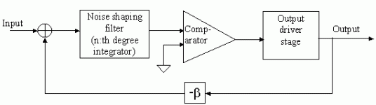
Bricolo said:In fact I asked for a basic schematic. No power/THD defined in it.
For a block schematic, I think the one I'm attaching here is useful.
A first order noise shaping filter (one integrating op-amp) is highly desirable to get good performance over the entire audio frequency range. Higher orders should be even better, but introduce stability problems. (Probably more problems than benefit for us at this point?!?)
The "output driver stage" contains the output filter as well.
By the way, I also like Bruno's idea of separating control/feedback from the output test mule
. The first PCB could be constructed with a line somewhere separating the parts, so you can chop off and replace one part later...If no-one else beats me to it (or protest), I will try to post an Eagle schematic tonight with a few proposals in place - to get something more concrete to discuss around.
Meanwhile, I would very much like to get suggestions on how the output driver stage should be constructed. I am familiar with circuits like IR2110, MAX626, HIP4080, and a few others in the same category. I like the IR2110 for the kind of output stage I have in mind, but I wouldn't mind switching it for some chip with a lower number of pins, a bit higher switching performance, possibly at the expense of lower voltage tolerance. (500V isn't needed here
)Or is the discrete driver from the UCD patent useful? (Haven't simulated/worked on it myself, so I don't know how it performs...)
Attachments
I think in this case the patent explains the operation very well, but you just can't visualize it, can you? That's what simulators are for, and I think "simulationable" should remain a design goal for that very reason.
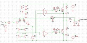
Your wish is my command !!!
Regards
Charles
Attachments
johanps said:
loop.gif
I don't see what causes de self oscillation in this diagram
That's the circuit BTW.
Transistors and FETs are the ones I just had on hand (i.e. my SPICE library). In real life there are of course better suited models available. Gate drivers were modelled as voltage controlled voltage sources.
The dimensioning (and ciruit) does of course leave much room for improvement.
Regards
Charles
Attachments
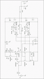
Uups, noticed that the "+" and "-" inputs are not marked on the comparator in that picture.Bricolo said:I don't see what causes de self oscillation in this diagram
Anyway, first ignore the noise shaping aspect (just think "amplification stage"). Then, if the momentaneous voltage on the output is lower than the input (times the feedback factor beta), that difference will be detected by the comparator, causing the output to go "high". This will quickly drive the output to a voltage slightly higher than the input (times beta), and so on... The mean value of the output will track the input. The precision with which it does so depends on the loop delay (i.e. the self-oscillating switching frequency, and the order of the noise shaping filter.
Bruno Putzeys said:
In the end I managed to order diamond coated burrs in a local shop (20 euros apiece or so. Manufacturer is called Pferd).
Like we say in french "Le monde est petit!"
Pferd's french "section" is 2 minutes far from where I live, and a member of my family used to work there!
They make great stuff
It's the whole smash: L1, C1, C2, R13, R12 plus the time delay from the comparator input to the power stage output.Bricolo said:If I compare your schematic to Johanps's loop.gif, I can't see the noise shaping filter (integrator).
Is it formed by C2 in the feedbacl loop?
JohanPSs loop is what we call a sigmadelta loop. You'll have to rearrange the blocks a bit (split the loop function, take the output halfway and add the input somewhere else) in order to "fit" the UcD schematic into that drawing.
The ingredients are the same but the recipe changes a bit. Or the recipe is the same but the ingredients change? Or both? Uhh never mind.
It's just a small detail, but:
I have no experience with comparators, but from the shematic it looks like an opamp with no (local) feedback, and some global positive feedback.
When using a diff pair on an amp's input, best results are obtained when both inputs see the same impedance to ground.
Shouldn't we match the impedances here too?
The reason why this is said for op amps is offset. The offset voltage of unmatched transistors (as in UcD) is so large it just doesn't matter.Bricolo said:When using a diff pair on an amp's input, best results are obtained when both inputs see the same impedance to ground.
Shouldn't we match the impedances here too?
That said, the production circuit is differential so impedance matching is automatically done.
phase_accurate said:That's the circuit BTW.
Transistors and FETs are the ones I just had on hand (i.e. my SPICE library). In real life there are of course better suited models available. Gate drivers were modelled as voltage controlled voltage sources.
The dimensioning (and ciruit) does of course leave much room for improvement.
Regards
Charles
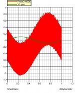
what did I wrong? mine simulates terrible...
Attachments
Bruno Putzeys said:
[snip] Interestingly, the exact properties of the ferrite material are not very important in gapped cores. Nearly all saturate at similar levels (300mT) and the inductance is determined by the air gap (effective mu << ferrite mu). Core losses are a different thing, but unless you're extremely unlucky it won't be a big issue.
So it really comes down to geometry.
Bruno Putzeys said:
That would provide some relief in the far field but the kind of dimensions we're talking about for a 100W amp (6x6cm?) is not "far field". The Q of the inductors would leave something to be desired because of their partial coupling, mutually and towards the ground plane.
I wouldn't settle for anything less than a closed magnetic circuit.
The reversed second wound air core configuration does have a near field emission problem. ;-)
Bruno Putzeys said:
These are either iron powder or ferrite. In the former case, they are invariably a "soft saturation" kind which produces tons of distortion even at low levels. In the latter case, an air gap needs to be ground in.
The cores Farnell has have no air gaps so some work is needed there too.
While trying to find info on how to machine ferrite I even heard large companies telling me it's impossible unless you have very specialised machines and tooling.
In the end I managed to order diamond coated burrs in a local shop (20 euros apiece or so. Manufacturer is called Pferd). They work fine for making air gaps in core halves. My drill stand, at 3000rpm is a bit slow though, which results in chipping.
For toroids I use grinding discs from Dremel (1mm thick or so) in a drill stand at slow speeds. It takes about 5 minutes to get through a toroid but it makes a clean cut.
Here is an idea concerning the acquisition of gapped ferrite toroids. For something like a 100 watt UcD, a DIY approach may be to use a couple of those clamp on EMI chokes as substitutes for gapped toroids. remove the toroid halves from their plastic retainers, add some type of separator between them for the gap, and then fasten them together with tape, wire tie, etc. Maybe for higher power, a few of those assemblies could even be attached in a row before threading windings through.
Bruno Putzeys said:
Quite precisely. That's why I think the most important thing is getting the comp/PS/filter done right. The control loop can be saved for last. You could even consider not placing the modulator on the same PCB with the power stage so you have a Universal Test Mule to try anything you like.
With this approach, the experimentation process appears much less tedious. It could be quite the opposite. Maybe a couple of universal power stages could be printed for circuit boards, one single and one bridge. They should be cheap so DIYers can afford to experiment with and blow them.
Hi,
Bricolo I can't see why it works at all. hmmm
Charles, how is the upper gate drive signal being level shifted to follow the load voltage in this?
Also, please do me the courtesy of explaining why you mixed the feedback signal with the input? Is that because of the lack of an inverting driver stage so it basically works exactly the same way?
If not I have no clue.
I think when it comes down to it, I prefer using the patended driver over anything like a driver IC. Probably easier to use, faster, just has to be optimised so the gate signals intersect like \/ rather than like /\ to minimise shoot through.
More importantly it demonstrates alot of the proper techniques for a discrete high speed half bridge driver and easily simulates!~
People would learn alot more by using that.
Regards,
Chris
subwo1 said:
With this approach, the experimentation process appears much less tedious. It could be quite the opposite. Maybe a couple of universal power stages could be printed for circuit boards, one single and one bridge. They should be cheap so DIYers can afford to experiment with and blow them.
Hi,
Or just singles that can easily be bridged, 1 size fits all.
....That could really liven up the experimenting you're right lol .
Regards,
Chris
- Status
- This old topic is closed. If you want to reopen this topic, contact a moderator using the "Report Post" button.
- Home
- Amplifiers
- Class D
- Development of a "reference" class D starting point