I've learned much about commercial designs in my Krell project. The KMA-160 combines all these things you guys are talking about ") The input is FET for high impedance, the voltage gain stage is all fast bipolars, then there's a MOSFET stage (with gain 0.5, not sure why they do that), to isolate the front end from the current gain stage. Finally there's a Sziklai driving the output. What would you call that? A Darlkai? A Sziklington?
The input is FET for high impedance, the voltage gain stage is all fast bipolars, then there's a MOSFET stage (with gain 0.5, not sure why they do that), to isolate the front end from the current gain stage. Finally there's a Sziklai driving the output. What would you call that? A Darlkai? A Sziklington?
So it seems you can eat your cake and have it, too. But it's going to cost you 72 transistors per channel.
The input is FET for high impedance, the voltage gain stage is all fast bipolars, then there's a MOSFET stage (with gain 0.5, not sure why they do that), to isolate the front end from the current gain stage. Finally there's a Sziklai driving the output. What would you call that? A Darlkai? A Sziklington?So it seems you can eat your cake and have it, too. But it's going to cost you 72 transistors per channel.
lumanauw:
What Parasound amp did that output stage come from?
Just curious ...
What Parasound amp did that output stage come from?
Just curious ...
lumanauw said:...
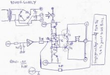
What about this output stage that I attach?
...
Here's an example of the topology I'm talking about. Although I think this design has one too many capacitors (I'd omit C9/R22), everything starting with Q4/Q5 and to the right of that is the same as the KMA-160:
From http://www.ampslab.com/c70.htm
An externally hosted image should be here but it was not working when we last tested it.
From http://www.ampslab.com/c70.htm
jwb said:then there's a MOSFET stage (with gain 0.5, not sure why they do that), to isolate the front end from the current gain stage. Finally there's a Sziklai driving the output. What would you call that? A Darlkai? A Sziklington?
It sounds like this sziklai has some gain to enable full voltageswing-
output. To prevent reversebiasing it make sense to half the max swing
before outputstage. This reversebiasing can be deadly and occurs
when amp is driven into clipping.
I would always add a predriver to a sziklaiout, or you get very reactive
loads to the vas.
What about Darsziklington ?
Mike
Hi, Mlloyd,
Oops, I forgot to mention. That CCT belongs to Mr. John Curl, with Parasound amp. The type is HCA.
Hi, Mr.Pass,
Thanks for the explenation. Having your advise is very rare nowdays.
Another question. Does having all Nch device for the output stage have great benefit compared to having NPN-PNP complementary output stage? All Nch will "behave" exactly the same up to very high frequencies (1hz-Mhz), while PNP will not behave exactly the same as NPN as the frequency rises, like GM said.
But in other thread, using All Nch gives problem, like with cross conduction.
For Sound Quality which is better audibly?
Complementary outputs are usually give a more linear result. Although using all NPN will mean same on resistances, capacitances, Ft, etc. they have to be driven in different modes which gives the upper and lower half different characteristics (both electrical and thermal).
Cross-conduction can occur in complementary as well as NPN output stages. Using all NPN can make it easier to avoid cross-conduction as then all you have to do is make the charge/discharge characteristics of the driver stage equal.
Cross-conduction can occur in complementary as well as NPN output stages. Using all NPN can make it easier to avoid cross-conduction as then all you have to do is make the charge/discharge characteristics of the driver stage equal.
MikeB said:
It sounds like this sziklai has some gain to enable full voltageswing-
output.
I just built a small 50W @ 4ohms amplifier, and I have to agree that the sziklai seems to drive the speaker a little harder than EF for the low voltage that I'm using to run my amp. (48V total)
I never used sziklai until I came across sound.westhost.com (Rod's site)
Overall, sziklai seems to be thermally stable in my experiences, but anyone that cares to comment on sziklai, please do so.
CFP allows more output voltage swing at the expense of saturating the output devices deeper and causing >10A cross-conduction pulses when exiting from clipping
This is particularly destructive at high frequencies >= 10Khz and high supply voltages
In general, the deeper the output devices get saturated when clipping, the longer it takes for them to recover from saturation. Classic EF output stages are almost free from cross-conduction issues since the VAS and the driver transistor saturate first
Clamping the VAS output to get some control over the amount of saturation of the output devices during clipping is advised when using CFP
In general, going for less than Vce=2V during clipping is a bad idea, particularly with high voltage bipolar transistors
Triple darlington provides less voltage swing since it usually clips 4 diode drops below supply rails [including VAS], but this ensures flawless behavior during clipping
CFP topology would be the perfect choice if output devices had zero base charge and instantaneous turn-off when drive is removed. But real world bipolars and MOSFETs require some time to get desaturated and turned off, and the process is similar for both : Extracting stored charge from some junction
QSC's grounded collector topology is not compatible with Common Feedback Pair since the collectors of the output devices are directly grounded instead of connected to a 'current feedback resistor' shared also with the emitters of the drivers, so there is no 'common feeback' at all
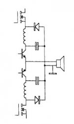
This sample schematic shows the basics of grounded collector topology
As it can be seen, the output devices are not working in common emitter topology, but in an 'inside out' emitter follower topology, since the collectors are connected to ground and the load is driven from the emitters through floating power supplies
Actually the drivers are the only devices working in common emitter since its emitters are effectively grounded [as its base current is wasted to ground and never reaches the load]
Furthermore, the current across the load is not sensed directly at the output devices, instead it's indirectly sensed at the emitter resistors of the drivers [points A and B] and properly scaled. A smart SOA protection is used, it does not allow more drive than required for any output voltage, and it also prevents the ouput devices to get deeply saturated during clipping, so cross-conduction problem is almost solved
So definitely this is not a CFP... Actually it has nothing to do with CFP
PD: The input op-amp is connected in such a stange way since it's driving an inverting output stage
This sample schematic shows the basics of grounded collector topology
An externally hosted image should be here but it was not working when we last tested it.
As it can be seen, the output devices are not working in common emitter topology, but in an 'inside out' emitter follower topology, since the collectors are connected to ground and the load is driven from the emitters through floating power supplies
Actually the drivers are the only devices working in common emitter since its emitters are effectively grounded [as its base current is wasted to ground and never reaches the load]
Furthermore, the current across the load is not sensed directly at the output devices, instead it's indirectly sensed at the emitter resistors of the drivers [points A and B] and properly scaled. A smart SOA protection is used, it does not allow more drive than required for any output voltage, and it also prevents the ouput devices to get deeply saturated during clipping, so cross-conduction problem is almost solved
So definitely this is not a CFP... Actually it has nothing to do with CFP
PD: The input op-amp is connected in such a stange way since it's driving an inverting output stage
Hi, EVA,
Nice analysis on grounded emitor (grounded collector) topology. Do you think this topology is the "right one" for making big rating power amp?
In your opinion, what is the bad-side of using this grounded topology?
QSC is famous for this grounded topology, but they also make CFP model, like CX1202, DCA3422. They use CFP with no problem, for such a big rating amp.
Sorry for the mistake, it's 'grounded collector'. I've corrected it and also corrected some mistakes in the schematic
I don't remember any schematic from QSC using CFP, I will try to get schematics for the models you mention
The obvious advantages I see in grounded collector topology are :
- No isolation is required between heatsinks and output devices, and no isolation is required between heatsinks and case/ground, so assembling is easier
- High voltage input stage and VAS are not required, a simple circuit with +-15V rails does the job instead
The disadvantages I see :
- Precise bias setting is not easy, these circuits tend to work in class B with some zero-crossing glitch, altough feedback corrects it pretty well below 1Khz
I have built and tested my own version of that circuit but somewhat modified. I used a triple darlington with the emitters of the output devices grounded through suitable current sharing resistors. The collectors of the drivers and the outputs were connected to floating power supplies and the output was taken from the center tap of the power supplies. The collectors of the predrivers were connected to a +-15V regulated supply and it's bases were driven from a discrete low voltage VAS and input stage also powered from the +-15V supplies. Bias was succesfully controlled with a classic Vbe multiplier
I used A1837/C4793 drivers and A1295/C3264 outputs, all with very high Ft since these circuits require fast devices
With that circuit I got mixed feelings :
- It was hard to fully remove parasitistic oscillations [initially I was trying to use too high a gain-bandwidth product, around 30Mhz]. Also, the triple darlington was oscillating by itself at up to 20Mhz until I added proper decoupling and common mode filtering to the floating supplies
- Clipping recovery was awful with lots of cross-conduction and ringing, until I added clamping diodes and drive current limiters to prevent the output devices and drivers from saturating at the expense of reduced output swing
- The input stage and the VAS were very easy to achieve, since with +-15V supplies there are no dissipation issues and no voltage limitations. I did everything with cheap BC550C/BC560C, featuring low noise, high gain and high Ft
I like this topology
Eva said:CFP allows more output voltage swing at the expense of saturating the output devices deeper and causing >10A cross-conduction pulses when exiting from clipping
This is particularly destructive at high frequencies >= 10Khz and high supply voltages
In general, the deeper the output devices get saturated when clipping, the longer it takes for them to recover from saturation. Classic EF output stages are almost free from cross-conduction issues since the VAS and the driver transistor saturate first
Clamping the VAS output to get some control over the amount of saturation of the output devices during clipping is advised when using CFP
Eva,
You can avoid cross conduction, and speed up Your CFP output stage, if put capacitor between the base of the output devices. 10-100nF works good, series with some 10ohms close to the base to avoid oscillation.
This capacitor helps to discharge the capacitance inside the output devices, and results no cross conduction. It works, I made measurements, and there was much less current increasing with high frequency square waves as without capacitor.
sajti
Hi Eva,
That was a neatly written explanation/summary.
The cross conduction arises when NFB loop boosted drive is faster than the previously conducting output half device can recover.
Sajti's suggested capacitor connection behaves like a reciprocating 'pull down' circuit for both output halves, and sometimes it is possible to connect an additional BC327/337 type of transistor of opposite polarity between output base/gate and emitter/source rail for even more speedy 'pull down' on a per-half basis.
Cheers ........... Graham.
Hi, EVA,
I like this grounded type also. Like you say, it allows good small signal transistor for differential and VAS even low voltage fets will work fine and without dissipation problem. The downside is that this topology will always have bigger OL gain (than the same topology with ordinary 3stage), because the output stage will always have gain.
Infact I tried to exploit this topology to a "single stage" power amp, which I attach here.
What do you think about it? (I've got one negative opinion about this idea from a reputable source).
It's kind of "current feedback" because input and feedback are injected to emitors of VBE multiplier. That means the value of Rinput and Rfeedback should be quite low.
And I doubt this idea can maintain 0DC, because the only point connected to ground is RG before the buffer.
I cannot eliminate the buffer, since the inputR and feedbackR will be low valued, needed big current. Direct signal from preamp is not strong enough for driving the point injected to VBE multiplier emitors.
Attachments
Sajti :
I remember your capacitor trick from previous posts. I've tried it in a couple of commercial 'load-tied-to-collectors' designs that were blown and I had to repair. Both showed strong cross-conduction when leaving clipping [up to 20A spikes per pair of output devices] and I tried 1nF, 10nF and 100nF, but I got little results except some ringing
One of the circuits was op-amp driven class B, showing clear zero-cross distortion above 1Khz. The output of the op-amp showed very big negative spikes when leaving positive clipping and vice-versa. Obviously these spikes were turning on very hard the other side of the output stage and this explains why the capacitor trick had little effect :
A saturated bipolar transistor allways takes longer to desaturate than an idle transistor to start conducting, [no matter how much negative base drive is applied]
Graham Maynard :
As you mention, the problem of cross-conduction is more likely to happen when the VAS tries to drive the output stage faster than it can react, and this demonstrates that CFP and it's variants are allways slower than emitter followers, and slew rate and clipping points should be limited to protect them from cross-conduction
In the other hand, I've designed a test EF circuit based in the same driver and output transistors as one of the commercial designs I repaired [BD139/BD140 TIP35/TIP36] and I got no measurable cross-conduction nor zero-cross distortion. I added clamping diodes to limit the minimum Vce of output devices to 2.5V for NPN and 2V for PNP and further speed-up clipping recovery and reduce recovery overshoot [PNPs appear to recover faster given the same Vce]
lumanuaw :
Your circuit may probably work, altough it will require more current gain than the one provided by a single BJT to be practical, and it may require also an additional VAS to get rid of the Vbe error of the output devices. But the only way to know is building, testing and expending hours witn oscilloscope and signal generator. Try it
But remember that floating-supply topology is only useful when the required output power is high [ie: >60V rails and high output current]. For 'exotic hi-fi' and lower rails, a classic EF is a much simpler [and probably better] solution since 65V BC546B/BC556B, 100V BD139/BD140 and 120V/150V japanese transistors show pretty decent specs
In contrast, my floating-supply amplifier attempt was intended to experiment with class-G or class-H modulated power suppy rails of up to +-150V, but a lot of work is still to be done
Hi, EVA,
I've built quite many amp with this topology, infact. But all that I've built is ordinary 3stages (differential, VAS, output=grounded type). They all sounds wonderful. I can say they sound better than ordinary 3stages power amp with similiar topology. I think this is mainly caused by 2 factors:
1. The differential and VAS works only from 15V. No heat problem here and I can use good small signal transistors. I use BC550-560, and can put big bias at VAS too
2. The VAS swings very little (only takes 0.6V to modulate the output to full on). This means the VAS has much smaller distortion compared to ordinary 3stages amp (which has to swing from 0 to full voltage). Minimum voltage fluctuation gives minimum distortion, isn't it.
Since you are investigating on class G/H, there is another "clever" solution provided to gain efficiency in big rating power amp. Class G and H still dissipate the heat in the rail modulator transistor itself.
In this idea, the rail is modulated by classD. It's from a Swiss' pro amp manufacturer (Labgruppen if I'm not mistaken)
The idea is very clever. The supply is modulated like output voltage by class D power amp, while the audio amp itself can be class B, AB or even class A.
I look at the principle, and to make it work, I think we will need 3 power amp. 1 is the main audio power amp (class B/AB/A), 1 is classD power amp for modulating positive rail (eg: always +5V than the output signal---working from 0 to +VCC) and 1 classD power amp for modulating negative rail (eg: always -5V from the output signal---working from 0 to -VCC).
Attachments
This moduladed supply rail technique is what I was calling 'class H'
I have some alternative ideas on this area, like allowing the positive rail to drop below ground and the negative rail to rise above ground to get true class-D efficiency with inductive loads and allow to use cheap TIP35/TIP36 operated at Vce=10V to produce more than +-100V output swing and >1200W@4ohms with just 3 pairs of output devices
I have some alternative ideas on this area, like allowing the positive rail to drop below ground and the negative rail to rise above ground to get true class-D efficiency with inductive loads and allow to use cheap TIP35/TIP36 operated at Vce=10V to produce more than +-100V output swing and >1200W@4ohms with just 3 pairs of output devices
- Status
- This old topic is closed. If you want to reopen this topic, contact a moderator using the "Report Post" button.
- Home
- Amplifiers
- Solid State
- Darlington and Triple darlington