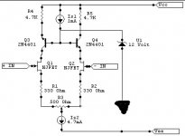
ppl said:When I first tried this Technique i got More DC offset with the Zener Grounded that returned to the current source. I must point out the Zener is only for Illistration a real Circuit would have a Quiet Precision Voltage reference.
???? Its the BOTTOM pin of the zener that needs to go to gnd, not the top one, that should stay at the current source. The way it is here will give you a HUGE offset.
Jan Didden
ppl said:The Pot Adjusts the DC offset. as for the sound the Voltage ref connected to the Current source vs Ground Produced a sound similar to what more Feedback dose.
Aha? You actually listened to this circuit?
Jan Didden
To answer EchoWars,
No, not a pot between the two emitters with wiper to supply, but rather a rheostat on the feed rail, supplying greater or lesser current to the DA as a whole.
I have my doubts about a trimmer pot across the emitters. This approach would certainly accommodate different Vbe on the two 'non-matched' devices; but it also means that each transistor sees different degeneration, and thus operates with different transconductance. I believe this is bad for the feedback network, which should see the same transconductance at its node as the input. I'm sure there is a math reason for this, too. Bam?
Cheers,
Hugh
Hugh, you know I cannot resist 
For Echo's circuit, call the transistors Q1 and Q2. Base voltages v1, v2; collector currents i1, i2, resistance between Q1 emitter and wiper R1, Q2 emitter and wiper R2, and wiper to supply R3.
Then, small signal,
i1 = (v1-v2)
. _________________________
. K1 - K2/(K2/R3 - 1)
Where K1 = R1+(1/gm1), K2 = R2 + (1/gm2)
sorry, I don't have an equation editor.
So the idea is to make the contribution to i1 equal between gm1 and gm2, to minimize distortion.
If R3 is infinite (perfect CCS) then the equation becomes:
i1 = (v1-v2)/(K1+K2)
And it is balanced provided R1=R2 and Ic1=Ic2 (because gm varies with i in a BJT). Otherwise things get complicated and imbalanced.
My recommendation, for minimum distortion, is to hand select the BJTs for equal Vbe and make R1=R2 and Ic1=Ic2. OR use JFETs which have more linear gm, BUT you then have to hand select the JFETs for equal gms. So you are stuffed either way.")
If R3 is infinite (perfect CCS) then the equation becomes:
i1 = (v1-v2)/(K1+K2)
And it is balanced provided R1=R2 and Ic1=Ic2 (because gm varies with i in a BJT). Otherwise things get complicated and imbalanced.
My recommendation, for minimum distortion, is to hand select the BJTs for equal Vbe and make R1=R2 and Ic1=Ic2. OR use JFETs which have more linear gm, BUT you then have to hand select the JFETs for equal gms. So you are stuffed either way.
Yes the Bottom Part of The Zener Grounded as you sugest. Regarding the Pot across the Sources of the Diff amp's jfets, If i understand AKSA correctly Removing the Pot and Use hand trimed Resistors in the Top half of the cascode Collector's?This Indeed sounds interesting. Oh Yes i have listened to the Zener Grounded and as connected and liked the more Cleen reproduction as connected rather than Grounded. The Key is the Voltage reference and Current source must be low noise or this gets injected through the sources of the J-FET's
No. I'd never use the circuit I posted. It might balance the pairs, but does nasty things to gain....and stuff.AKSA said:To answer EchoWars,
No, not a pot between the two emitters with wiper to supply, but rather a rheostat on the feed rail, supplying greater or lesser current to the DA as a whole.
I have my doubts about a trimmer pot across the emitters. This approach would certainly accommodate different Vbe on the two 'non-matched' devices; but it also means that each transistor sees different degeneration, and thus operates with different transconductance. I believe this is bad for the feedback network, which should see the same transconductance at its node as the input. I'm sure there is a math reason for this, too. Bam?
Cheers,
Hugh

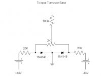
If all I wanted was to remove DC offset, I could connect the circuit below to the base of the feedback resistor. But I suspect that a current source at the emitters may offer more benefits than negatives, and I'd certainly like to try it.
Attachments
Based on Traderbams work, it appears that the resistors need to be matched as well. For a fully complementary-symmetry design, to get the theoritical second order distorition cancellation, everything has to be matched - transistors as well as resistors. In practical terms, the resistors need to be matched at least as good as the transistors, and probably be much better matched to remove them as a practical source of error. I mean, if you can match beta/Vbe to 1%, then the resistors should probably be matched to better than .5%, even .1%.
Does this make sense?
Does this make sense?
Matching
Hi,
The differential amplifier works by virtue of the two halves of the pair being perfectly matched. You can match transistors or FETs by hand using a selection process but I believe you will not come closer than 1-2%.
If you are using a monolithic dual like f.a. MAT02 or 2SK389 or 2N5912 the transistors are inherently matched also when they heat up as they are in very close thermal contact. The latter is not the case if you glue two transistors together and surround them in aluminium.
As my first steps in audio were repairing complementary designs like the GAS Ampzilla power amplifier I have experience in matching. A problem arises with a full complemenatry frontend as you now need four matched transistors of opposite polarity. (two NPN and two PNP, all being equal)
First I was so naive thinking that I would find a chip with four equal transistors like the MPQ6002 but it proved that the NPN had much larger current gain. So with a complementary design you never get it perfect. I also thought of MAT02 and MAT03 but the gain or Beta is not the same. The situation with FET's is even worse as pictured above in an other post.
Another problem arises with the full complementary design as there is no P-channel alternative for the 2N5912. So in my preamp I gave up and designed only for the complementary ouputbuffer. For the poweramp I still want to design I have not made up my mind. I like FETs at the input but if it must be complementary I can only use 2SK389 and and 2SJ109 like John Curl and Erno Borbely.
Michael I hope I answered a little bit your question.
Jfet matching
The J109 and K389 pairs spec matching at 0.9 for Idss and transconductance. Matching K170s and J74s closer than this is not very difficult but is more time consuming. Very good thermal tracking can be achieved by mounting the flat faces together with a drop of heat sink compound and using a small rubber O ring. I have seen this technique used by Steve McComick in his products.
Differences between N channel and P channel gains can often be corrected by adding more degeneration to the N channel pair as it most often has higher transconductance.
I am having trouble understanding why, in a complementary-symmetry design, the top and bottom diff amps have to have transinstors matched for gain and Vbe. Each each section, yes, of course. Clearly the NPN sections and the PNP sections, each half thereof, need to be tightly matched to approach theoritical operation. But, the top and bottom halves don't seem to be related. I mean, they each amplify and output a signal to their own VAS. The VAS thus isolates the outputs from each half. As long as the gains of the DA stages are matched - and can't this be accomplished via the resistors - should not close to ideal performance be obtainable (at least at a single temperature)?
In other words, if we make the open loop gains of the top and bottom DA stages identical, down to .1% or better, using the resistors, does it then really matter if the betas and Vbe's of the NPN's match those of the PNPs?
In other words, if we make the open loop gains of the top and bottom DA stages identical, down to .1% or better, using the resistors, does it then really matter if the betas and Vbe's of the NPN's match those of the PNPs?
Matched transistor Pairs
I have found that for BUT's the LS-352
http://www.linearsystems.com/ and LS-312 make a Nice Complimentry pair of matched Dual Complimentry transistors
I have found that for BUT's the LS-352
http://www.linearsystems.com/ and LS-312 make a Nice Complimentry pair of matched Dual Complimentry transistors
Jeff,
I agree with you.
Can't see why you'd bother matching top and bottom Vbe/beta for both halves of a complementary symmetrical design.
Any more, in fact, than you'd match the NPN and PNP of a single output pair on a power amp. That always struck me as a nonsense as well......
Cheers,
Hugh
I agree with you.
Can't see why you'd bother matching top and bottom Vbe/beta for both halves of a complementary symmetrical design.
Any more, in fact, than you'd match the NPN and PNP of a single output pair on a power amp. That always struck me as a nonsense as well......
Cheers,
Hugh
I agree too.
Matching the differential transconductance between the two halves is important, but the vbe and betas should not be very important. One thing that can be important, especially with high feedback designs, is the differences in capacitance between npn and pnp devices. This is trickier to deal with.
Again I think a single diff pair will be the least of you distortion worries provided the dynamic ic is << static Ic. In some low/no feedback circuits with certian VAS stage designs you can end up with quite large current swings in the diff pair; this is a case where having symmetrical diff pairs may help overall. I think Krell do this and use JFETs whereas Naim use single BJTs.
Bam
Bam and Hugh,
I have always found that full comp designs tend to have a shallow (depressed) midrange campared to a single ended design. Peter Moncrieff of IAR used to call this midrange suckout.
I have always wondered if this was due to the reduction of second order distortion products and more higher order components in comarison to a single ended design.
What are your thoughts?
Regards,
Jam
- Status
- This old topic is closed. If you want to reopen this topic, contact a moderator using the "Report Post" button.
- Home
- Amplifiers
- Solid State
- Current Regulator Diodes (CRD) - Why Seen So Seldom?