Hi, Steven,
Thanks alot for the cct . I will try to understand it better, but for now it seems that what makes non-turnoff in the Hans Hartsuiker cct is the existence of R21-R31 (220k). Without them, the output stage will turnoff.
I read that Blomley type of amp using "cut and paste" for each half of positive and negative signal. What happens if the "paste" part is not exactly in phase, will it result in another distortion (while it can eliminate turn-off distortion)?
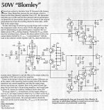
This Blomley generated cct are smart. My big question now is, why is it not so popular? I never see commercial unit using this approach. Is that output stage Xover distortion is not important?
Hi, PMA,
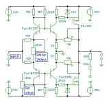
Thanks for the cct. T1-2-5-6 reminds me of NP-PMA, but the arrows are in different direction.
Some designers do not like current mirror, they say it is bad for sonics. While using this type of output stage, big chance it has to use current mirror.
How true is it that current mirror can ruin sonics? Is it only the case if it was put in differential, or it was for everywhere in audio cct, that current mirror is not suitable.
Thanks alot for the cct
. I will try to understand it better, but for now it seems that what makes non-turnoff in the Hans Hartsuiker cct is the existence of R21-R31 (220k). Without them, the output stage will turnoff. I read that Blomley type of amp using "cut and paste" for each half of positive and negative signal. What happens if the "paste" part is not exactly in phase, will it result in another distortion (while it can eliminate turn-off distortion)?
This Blomley generated cct are smart. My big question now is, why is it not so popular? I never see commercial unit using this approach. Is that output stage Xover distortion is not important?
Hi, PMA,
Thanks for the cct. T1-2-5-6 reminds me of NP-PMA, but the arrows are in different direction.
Some designers do not like current mirror, they say it is bad for sonics. While using this type of output stage, big chance it has to use current mirror.
How true is it that current mirror can ruin sonics? Is it only the case if it was put in differential, or it was for everywhere in audio cct, that current mirror is not suitable.
Hi Steven,
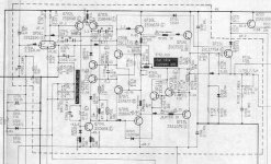
Hans Hartsuiker states that there are no output emitter followers, yet the outputs are complementary driven by BD139/140 drivers using common 0.56 ohm emitter resistors for local voltage feedback. These output halves are slow, hence the 10k/100pF input/NFB filtering and the ! undamped ! 20uH series output choke. This would not sound good by today's standards.
Hi Pavel,
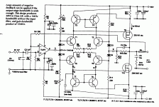
There are several aspects of your posted 'IH' circuit that I like.
1. the output device gates are pulled down as well as turned on,
2. the output stage should be faster than the filtered input,
though the input filter could be quite a load for older pre-amps,
3. fuse resistance is used to give a degree of error correction.
The fuse type should have been stated as there can be quite a
difference between types, and optimum operation is likely within
a narrow resistance band with specified wiring layout wrt
the 20 milliohm series output bias sensing resistors.
Hi lumanauw,
Sure ! ICs use current mirrors, and audio is full of ICs. Besides, the transistors you mention are not just mirrors but clever differential sensors.
I think that the manufacture of these types of circuits would need to be very exact for good results - with individual device characteristic optimising for good results, as Pavel is presently achieving.
Cheers ........... Graham.
Cheers ............ Graham.
Hans Hartsuiker states that there are no output emitter followers, yet the outputs are complementary driven by BD139/140 drivers using common 0.56 ohm emitter resistors for local voltage feedback. These output halves are slow, hence the 10k/100pF input/NFB filtering and the ! undamped ! 20uH series output choke. This would not sound good by today's standards.
Hi Pavel,
There are several aspects of your posted 'IH' circuit that I like.
1. the output device gates are pulled down as well as turned on,
2. the output stage should be faster than the filtered input,
though the input filter could be quite a load for older pre-amps,
3. fuse resistance is used to give a degree of error correction.
The fuse type should have been stated as there can be quite a
difference between types, and optimum operation is likely within
a narrow resistance band with specified wiring layout wrt
the 20 milliohm series output bias sensing resistors.
Hi lumanauw,
Sure ! ICs use current mirrors, and audio is full of ICs. Besides, the transistors you mention are not just mirrors but clever differential sensors.
I think that the manufacture of these types of circuits would need to be very exact for good results - with individual device characteristic optimising for good results, as Pavel is presently achieving.
Cheers ........... Graham.
Cheers ............ Graham.
Hi Lumanauw,
You're correct. R21/31 take care for a minimum current through the output devices.
Hi Graham,
I've done no simulations, neither did I build it, but I think the output stage of Hans is not that slow. It is a current mirror output with a gain of 1000 (yes, the 56R resistors in the diagram should be 0.56 Ohm). Current mirrors are normally quite fast. A 1 to 1 mirror has a cut off of fT/2 iirc, but I'm not sure how this is affected by the gain in the mirror. Anyway the transistors used are quite fast. The now discontinued Philips BDT87 and BDT88 have an fT of 70MHz (again iirc). Also the BD139 and BD140 are fast (for such old transistors).
Steven
After studying the smart cct's contributed by everybody, I come up to a simple conclusion, that non-turnoff can be easily made (without sophisticated cct's) by making a final stage a "Current Mirror with Gain". This is very obvious in Blomley cct.
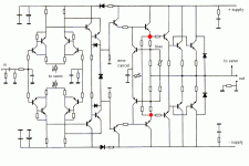
Here I attach a CCT by SonnyA. This is a Diamond buffer cct. Q15+R24 is current mirror+gain to Q17+R25.
I think this Diamond Buffer will never turnoff during all condition.
If Q15 never turns off, then Q17 will never turnoff also. Q15 never off here, it is always forced by CCS Q14, this means the finals Q17-18 never turnoff.
Attachments
Hi Lumanauw,
Sorry, but Q17 and Q18 can be cut-off easily. Your circuit does not operate as you think or intend.
The problem is that Q15 and Q17 are not a current mirror, neither are Q16 and Q18. Do a simulation and you will see that when the load current is big enough, the voltage drop across R26 or R27 will be so big that the opposite transistor will cut off. Your circuit keeps a constant bias voltage between the bases of Q17 and Q18, dependent on the current of Q10. This current generates a certain Vbe for Q15 and Q16, plus a constant voltage across R24 and R25.
Only if you make R24, R25, R26 and R27 zero, you will get a closed loop of Vbe's, a translinear circuit. Then I(Q15)*I(Q16)=I(Q17)*I(Q18), and because I(Q15) and I(Q16) are fixed by the current source, this results in I(Q17)*I(Q18)=constant. Now, if I(Q17) rises because of load current, through Q18 the reciprocal current value will flow. And I(Q18) will never reach zero, because IQ(17) will never become infinite. Please note that this ideal case is only valid when all junction temperatures of Q15-18 are equal and the transistors have an ideal exponential behaviour. The use of emitter resistors spoils the exponential behaviour.
Steven
Hi, Steven,
Thanks for the explenation. (You are good with electronics).
So, the same diamond buffer will not turnoff if we make R24,25,26,27=0?
I'm still curious about how Hawksford EC can maintain non-turnoff. Is it because the bias cct is separated by 2? One for positive signal and one for negative signal? And each other is independent in giving minimal VBE to final stage?
Thanks for the explenation. (You are good with electronics
). So, the same diamond buffer will not turnoff if we make R24,25,26,27=0?
I'm still curious about how Hawksford EC can maintain non-turnoff. Is it because the bias cct is separated by 2? One for positive signal and one for negative signal? And each other is independent in giving minimal VBE to final stage?
lumanauw said:I'm still curious about how Hawksford EC can maintain non-turnoff.
I am as well. I've attached an LTSpice simulation of the output stage of Cordell's error correction circuit from the AES Journal. It does have different supply voltages than Cordell's circuit. Running the simulation shows that the inactive device cuts off the same as a conventional circuit. The difference between the output stage gate voltages is almost constant with time, also the same as a conventional circuit. For turnoff to be prevented, the gate voltage difference must increase as the absolute value of the output current increases.
i'm sorry, i dont need itthanh said:if output transistors never turn-off but iq is more than 50mA , i still need that technique
Hi Lumanauw,
These kind of circuits are ratcher difficult to grasp because they are not very straightforward. At this moment I don't want to spend much time on it and don't start a simulation. At first glance it seems a non switching bias circuit to me, but maybe it is even doing error correction.
What amplifier is this circuit from? You seem to have a big collection of amplifier schematics.
Steven
lumanauw said:
I'm still curious about how Hawksford EC can maintain non-turnoff. Is it because the bias cct is separated by 2? One for positive signal and one for negative signal? And each other is independent in giving minimal VBE to final stage?
This remark about non-switching behaviour of the Hawksford EC circuit may well come from me. I think I have mentioned it once in one of my posts. It was what I remembered from the time that I was designing and building an amplifier with it (1983, >20 years ago). I know I had to make the emitter resistors of the output transistors rather small because when the voltage drop across one of these resistors becomes so big that the opposite transistors gets reverse biased then the error correction circuit suddenly stops working. So it is important to stay within the range that none of the output transistors ever is reverse biased. I admit this is not exactly the same as non-switching. The Vbe of the opposite transistor may reach 0V and at that moment the current through that transistor has stopped flowing. But the worst switching behaviour in amplifiers happen when the opposite transistor is becoming reverse biased and this is something that is not allowed to happen in the Hawksford circuit.
Looking at the circuit below: the voltage between the red nodes is more or less constant, and the voltage drop across the output emitter resistors (at full load current) may not cause this voltage to increase, as would happen by pulling the output outside the voltage window between the red nodes.
Steven
Attachments
- Status
- This old topic is closed. If you want to reopen this topic, contact a moderator using the "Report Post" button.
- Home
- Amplifiers
- Solid State
- Crossover distortion