Hi Don,
Was just scrubbing up in the bathroom and it occurred to me that I had read the term 'sliding bias'. Sliding bias is where the bias at the output stage is automatically adjusted either by input waveform or by output stage/load sensing, and there tends to be a delay which affects transient capabilities.
I feel that my stage is a 'sliding gain' circuit, with a gain characteristic that is pre-settable by resistor selection to increase with increasing load current demands, which is why I mentioned Mosfet like capabilities; i.e. the deeper the loudspeaker impedance dip - the greater the output current, yet without having all the usual phase shift and gain constantly arising, which could then need stabilising and lead to the inductive hf output characteristic so often observed with non-class-A NFB amplifiers.
Cheers ............ Graham.
Hallo Graham Maynard
i am just going to see pavel's amp
Hallo smoking-amp
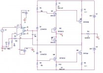
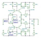
here I attach a simple amp with non-linear vas (look at schematic)
in simulation i got undistorted sine of amplitude of 27.5V
with idle current as 'low' as 1.34A the output mosfets are never turning off.

do you feel it is considerable gain of efficiency compared to pure class A (maybe it wolud be good only to make xover dist. softer in AB) or just slight???
just first trial... maybe after little development......??
looking forward to seeing your opinion
i am just going to see pavel's amp
smoking-amp said:
If I understand your idea correctly, you are trying to get a non-constant voltage between the upper and lower output transistors to perform sliding bias by means of two separate VAS circuits? The required variation of bias for sliding bias is fairly small, I think, so it would be difficult to get sufficiently accurate tracking between the two VAS circuits, especially with nonlinearities in each.
Hallo smoking-amp
here I attach a simple amp with non-linear vas (look at schematic)
in simulation i got undistorted sine of amplitude of 27.5V
with idle current as 'low' as 1.34A the output mosfets are never turning off.
do you feel it is considerable gain of efficiency compared to pure class A (maybe it wolud be good only to make xover dist. softer in AB) or just slight???
just first trial... maybe after little development......??
looking forward to seeing your opinion
Attachments
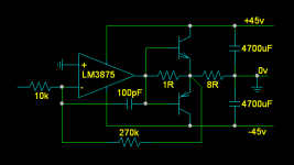
This cct is drawn by Circlotron. It intended for other purpose, but I see an interesting possibility.
If the gainclone is free of xover distortion. The transistors are on only if the drop in 1R reaches 0.6V.
So, the transistors do on-off, but the small signals are provided by the gainclone.
Is xover distortion occurs here or not when the transistors are on and off?
If the gainclone is free of xover distortion. The transistors are on only if the drop in 1R reaches 0.6V.
So, the transistors do on-off, but the small signals are provided by the gainclone.
Is xover distortion occurs here or not when the transistors are on and off?
Attachments
non-linear VAS
Hi darkfenris,
Brain cells are smoking here analyzing your circuit, I should put it on the simulator to see for sure. Seems to me (looking at M1, M2 side) that the sequence of two grounded source circuits will give the product of the two square law transfers of each. The bias pot(s) will linearize one of them somewhat however. The M3 mosfet I suspect is intended to increase non-linearity further, but I think it doesn't do much except maybe compensate DC output offsets. My reasoning here is that the M1 mosfet already has this same non-linearity built into its gate/source, so is just adding more of the same effect. Would have to try on the simulator, an open loop voltage to current plot to see if this is true.
Never the less, the near 4th power transfer of M1 and M2 cascaded will give something like a 3rd power variation of transconductance at the output. Putting the two sides together in complementary fashion then sums two of these non-linearities with a parabolic like resultant.
Seeing that it takes 1.34 A to get good results (half way to class A maybe?), maybe need to use a different order non-linearity? I would try bipolar transistors in M3/M4 or even any of the other pair locations just to see what results are, maybe can lower idle current then with some combination.
The other issue that would concern me would be the thermal stability of idle current setting since there is considerable gain after the bias setting adjustments. Maybe have to resort to some kind of servo to hold steady.
Someone maybe should do a simple math study of what type non-linearity sums best in complement fashion to a give smooth curve. Maybe it is not high order non-linearity, but rather something just over linear, like 1.1 power say. Have never seen anyone work this out.
On the gain clone idea, I would think it would work better with some Vbe bias network for the transistors. There has to be some kink in the transfer curve when they suddenly turn on.
Hi Graham,
I think Lumanauw has come up with the best example of the class H amp I described, with the Technics amp. Some class H use separate varying rails, maybe a pair of PWM switchmode supplies even. I would be curious to know why Technics dropped this design, my first guess would be cost considerations, it is using twice as many high power parts as normal.
Don
sliding gain
Hi Graham,
Yes, my mistake on calling your circuit sliding bias, your design is definately in the fast sliding gain or varying transconductance class. I was being too loose in my meaning of sliding bias, as these usually entail a more slowly varying bias level following the signal envelope.
One fast varying transconductance design not mentioned so far is the Linear Technology LT1166 IC chip. This controls the upper and lower stage currents so their product is a constant. Usually I hear comments about it not working well at the high frequency end however. Perhaps LT needs to come out with a faster version, or some have commented on the need for a geometric mean control rather than a product rule. A less power conserving rule, but more smoothly varying current transition.
Don
experiment
I have been meaning to try a little experiment on the LT1166 chip sometime, but never seem to get around to it. Maybe one could put an RC network on the inputs to the chip to keep out high frequencies, so it would effectively rely on using the last computed bias as a fixed bias level for high frequency zero crossings.
Since the high audio frequencies tend to be lower in amplitude and their harmonics often above the audible range anyway, this might be a pretty good fix. It will have the effect of using a slightly higher bias for high frequency zero crossings, since it will be using a bias previously computed at a higher output level. So it would just be nulling out some tiny power saving effects when high frequencies cause zero crossings. Not a bad thing, since the MOSFEToutputs will be operating with a little higher transconductance then, which will help with their high frequency slew rate. Might actually be a nice improvement. LT, you can send me a bonus for this if it works! (fat chance)
Don
Hi Lumanauw,
"How is the xover distortion in mosfet output stages? ...."
I cannot really add much to what I have read in Self's book on this. I think the output MOSFETs with class A thing comes from the fact that the complementarily varying transconductances add up to a constant for square law devices in class A configuration.
Self doesn't seem to like the fact that MOSFETs don't have a sharply optimal bias point for class aB, but their crossover just gets better smoothly as the idle current is set higher. I don't really see any big problem with that, at least one can adjust it to ones pocket book for heatsinks and electric bill.
The one area where I think there could be an advantage for MOSFETs would be in using a Hawksford style error correcting output design, where their typically greater speed is an advantage for the local feedback loop performance.
Self doesn't seem to like the fact that MOSFETs don't have a sharply optimal bias point for class aB, but their crossover just gets better smoothly as the idle current is set higher.
I think there is a further significant advantage that goes along wiyh this this. If far as I can tell, a small drift in the bias setting changes little in a MOSFET output stage, whereas, a similarly small drift in a BJT stage (particularly if CFB) can degrade the distortion performance fairly significantly.
Re: sliding gain
Having (far as I know) invented the term, it properly refers to
a bias circuit which responds to the actual waveform, not its
envelope. It might be that there are such beasts out there,
but I haven't seen any unless you want to count the Krell
"sustained plateau" biasing, which technically does not follow
the envelope, but is triggered by it.
Also, a sliding bias circuit, as with mine or Hawksford's
( or Cordell), is be extremely fast, and is not a source of
transient distortion at audio frequencies.
smoking-amp said:Yes, my mistake on calling your circuit sliding bias, your design is definately in the fast sliding gain or varying transconductance class. I was being too loose in my meaning of sliding bias, as these usually entail a more slowly varying bias level following the signal envelope.
Having (far as I know) invented the term, it properly refers to
a bias circuit which responds to the actual waveform, not its
envelope. It might be that there are such beasts out there,
but I haven't seen any unless you want to count the Krell
"sustained plateau" biasing, which technically does not follow
the envelope, but is triggered by it.
Also, a sliding bias circuit, as with mine or Hawksford's
( or Cordell), is be extremely fast, and is not a source of
transient distortion at audio frequencies.
Hi Nelson,
OK! I'll consider that as authoratative on the matter.
This brings up the question as to whether their is really any difference between the terms sliding bias, sliding gain, and sliding transconductance when operating at signal speed. Maybe just semantics as to how the particular circuit appears to operate to 1st order? Voltage feedback or current feedback.
"to be extremely fast ... no transient distortion..."
Perhaps this is the problem with the LT1166 chip, not fast enough to avoid messing up global feedback stability. I wonder what effect putting an RC lowpass filter on the LT1166 chip inputs might have in the transistion region where its local loop phase is at quadrature with the signal.
Don B.
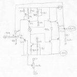
In a differential (without RE) we have 2 emitors tied together, and 1 other path to the CCS. It works fine here. Kind of Y intersection. 3 current paths here.
In EC, we have 2 transistor for setting VBE by connecting emitor to emitor, directly. And nothing between them. And no other path. It is one way current path where emitors are tied together without RE.
Some who uses EC found oscilation, and put small C (pf) from these junction of emitor-emitor in EC VBE multiplier to ground, to stop oscilation.
I accidently made an experiment like I attached, I uses emitor heading emitor in Q1 and Q2. It is big current here, making the effect more obvious.
This emitor heading emitor without RE or without other current path INDEED makes oscilation. Very visible in scopes. I can eliminate it by putting 100R between emitor of Q1 and emitor of Q2.
So, I have suspicion about heading emitor to emitor without RE in a one way current path, that whatever mechanism there is, is making oscilation.
This can be eliminated by putting RE, but unfortunately, in EC, the drop of this 2VBE is the reference point. In EC we cannot put R between emitor-emitor since it will change the whole voltge balance, becomes current depended.
NP, as the author of smart-bias, knows something about this. He put another diode between emitor-emitor junction, so the reference is about 3 times diode drop. Can be seen in his patent.
What is the mechanism of emitor heading emitor in one way current path that makes oscilation? Can it be eliminated by NP way, putting diode (non current dependant voltage drop) between emitors? Or it needs a current dependant voltage drop device, like 100R or other resistor value?
Attachments
to this, in the later models.
The later models does not incorporate smart-bias scheme, only ordinary VBEmultiplier with 2x4k7 attached to output.
Is it sonic consideration or stability consideration, or what, that makes this change?
Unfortunately, Mr. Pass as the author doesn't seem to want to comment this
The later models does not incorporate smart-bias scheme, only ordinary VBEmultiplier with 2x4k7 attached to output.
Is it sonic consideration or stability consideration, or what, that makes this change?
Unfortunately, Mr. Pass as the author doesn't seem to want to comment this
Attachments
Hi darkfenriz,
Can your circuit cope with +/- line voltage fluctuations and power output induced supply rail voltage drops ? Try this if you can simulate it.
I remember seeing something like this where the series resistor supplies to the IC were beneficially capacitor bootstrapped from the output emitters so that a lower voltage IC could control high power output.
Hi lumenauw,
Circlotron's circuit has an awful hf/dynamic audio response. Indeed it probably was not designed for audio.
For audio the 100pF capacitor would need to be reduced to 4.7pF or 2.2pF
Hi Don,
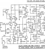
This attached circuit has a non-crossover near straight line transfer characteristic, even without NFB. It is due to Ian Hegglun and was published in Electronics World. It operates on the difference of two squares principle.
I once built something like the Circlotron circuit and NFB around the op-amp plus output devices did an excellent job of minimising crossover distortion.
It is possible to reduce the hf input of an amplifier, but the NFB loop must still operate at much higher frequencies for error correction, so the LT1166 might still be found wanting.
Cheers ............ Graham.
Can your circuit cope with +/- line voltage fluctuations and power output induced supply rail voltage drops ? Try this if you can simulate it.
I remember seeing something like this where the series resistor supplies to the IC were beneficially capacitor bootstrapped from the output emitters so that a lower voltage IC could control high power output.
Hi lumenauw,
Circlotron's circuit has an awful hf/dynamic audio response. Indeed it probably was not designed for audio.
For audio the 100pF capacitor would need to be reduced to 4.7pF or 2.2pF
Hi Don,
This attached circuit has a non-crossover near straight line transfer characteristic, even without NFB. It is due to Ian Hegglun and was published in Electronics World. It operates on the difference of two squares principle.
I once built something like the Circlotron circuit and NFB around the op-amp plus output devices did an excellent job of minimising crossover distortion.
It is possible to reduce the hf input of an amplifier, but the NFB loop must still operate at much higher frequencies for error correction, so the LT1166 might still be found wanting.
Cheers ............ Graham.
Attachments
Hi lumenauw,
Had a delay in e-mails/internet (was the solar wave/aurora responsible?).
Surely in your Post 52 circuit the shunt feedback requires a fixed voltage reference point for the emitter of the first transistor, thus adding series connected junctions and somewhat floating Q2 impedance merely increases non-linearity and dc instability ?
Post 53 shows clever output biasing within a closed global NFB loop.
Post 54 shows more conventional output biasing, but there is no global NFB.
Yes this will have a sonic impact because the NFB sensing comes from the VAS/ouput driver interface only, such that output voltage will be determined more by loudspeaker reactivity than the audio signal waveform. When this circuit drives a composite loudspeaker there is potential for the output voltage to say the tweeter, to become back emf modulated by phase shifted current flow due to bass/mid crossover/driver reactivity. Any different effect would be most audible upon transients, but whether one circuit or another sounds more correct than the other in the first place can only be determined by real life audition. I suspect that this circuit will have an unusual output impedance characteristic.
Cheers ............ Graham.
Hi, Graham Maynard,
Pardon me, but what is "shunt feedback"?
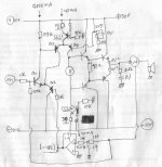
The cct on post #52 comes from a naif thinking that VBE is always constant, like 0.6V (In real world, it dont work like that). Learning that differential cancels harmonics, I came up with this idea of front end that is not differential (3 current path) but with a single current path, so I hope it doesn't cancel harmonic at all.
So, Q1 has ground point via 47k, and if we set Q2's base (by VR) at -1V2, we will have 0V at output.
But this design has no temp compensation at front end, the DC offset runs wild in the prototype. For improvement I come up with this design I attached, Q1 is replaced by CFP-like configuration (with Q3) and reference for Q2 is done by servo. In real life experiment this cct doesn't work good enough for audio amp
The point with this design is not the design itself, but I want to say what I found, that in single current path, and there is emitor headed to emitor, it gives oscilation.
What causes this? If this problem can be eliminated, Hawksford EC and NP's smart bias (that counting on this emitor headed with emitor for EC) surely fixes the output stage xover distortion.
Surely in your Post 52 circuit the shunt feedback requires a fixed voltage reference point for the emitter of the first transistor, thus adding series connected junctions and somewhat floating Q2 impedance merely increases non-linearity and dc instability ?
Pardon me, but what is "shunt feedback"?
The cct on post #52 comes from a naif thinking that VBE is always constant, like 0.6V (In real world, it dont work like that). Learning that differential cancels harmonics, I came up with this idea of front end that is not differential (3 current path) but with a single current path, so I hope it doesn't cancel harmonic at all.
So, Q1 has ground point via 47k, and if we set Q2's base (by VR) at -1V2, we will have 0V at output.
But this design has no temp compensation at front end, the DC offset runs wild in the prototype. For improvement I come up with this design I attached, Q1 is replaced by CFP-like configuration (with Q3) and reference for Q2 is done by servo. In real life experiment this cct doesn't work good enough for audio amp
The point with this design is not the design itself, but I want to say what I found, that in single current path, and there is emitor headed to emitor, it gives oscilation.
What causes this? If this problem can be eliminated, Hawksford EC and NP's smart bias (that counting on this emitor headed with emitor for EC) surely fixes the output stage xover distortion.
Attachments
hi Graham
my circuit was just an idea of using mosfet's natural nonlinearity to make a nonlinear vas and save out some idle current while keeping output mosfets never turning off (this sentence was too long )
I don't see the problem with fluctuating rail because i used zeners which makes this circuit a bit different from some 'similar'.
Also i wouldn't worry about thermal issues- twice a negative thermal coefficient isn't actualy positive coeficient.
But once more - it was just an idea and i hardly can imagine this working in real life because of:
1.choosing suitable (and very similar) mosfets combined with opamp-problems with 'low' current driving huge capacitance
2.If i would've chosen low-signal mosfets: do they have 'desired' nonlinearity
3.setting the biasing, i mean making vas mostefs at the border of conducting huge currents to get this non-linear effect (near border of Vgs), choosing suitable zeners - this all was a nightmare even in simulation (i cannot count how many times i got several volts voltage drop on 0.1 source resistors)
so...
stop asking me about details
start using mosfets as non-linear resistors -personaly i see much hope in it.
cheers
and thank you for nice conversation
have a nice day
dislike i have
my circuit was just an idea of using mosfet's natural nonlinearity to make a nonlinear vas and save out some idle current while keeping output mosfets never turning off (this sentence was too long
)I don't see the problem with fluctuating rail because i used zeners which makes this circuit a bit different from some 'similar'.
Also i wouldn't worry about thermal issues- twice a negative thermal coefficient isn't actualy positive coeficient.
But once more - it was just an idea and i hardly can imagine this working in real life because of:
1.choosing suitable (and very similar) mosfets combined with opamp-problems with 'low' current driving huge capacitance
2.If i would've chosen low-signal mosfets: do they have 'desired' nonlinearity
3.setting the biasing, i mean making vas mostefs at the border of conducting huge currents to get this non-linear effect (near border of Vgs), choosing suitable zeners - this all was a nightmare even in simulation (i cannot count how many times i got several volts voltage drop on 0.1 source resistors)
so...
stop asking me about details
start using mosfets as non-linear resistors -personaly i see much hope in it.
cheers
and thank you for nice conversation
have a nice day
dislike i have
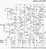
output stage always on
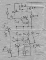
Here's what I think at this moment. We can still use ordinary VBE multiplier (since it has proven reability), so we have to push the non-off action outside VBE multiplier.
Q1 is VAS transistor, Q2 is VBE multiplier. From VBE multiplier to output stage is bridge by 2 of 1k resistor.
For making it simple, lets assume these 1k resistors from VBE multiplier are not there. I also draw not using drivers, to make it simple look.
Output stage is Q7-Q8, with RE=0.22ohm. With ordinary VBE multiplier in class AB, one of these transistors are on when the other is off
Assume there are 2 pairs of output stage. I put a sensing resistor in the collector of one output stage transistor. That is the 68ohm resistor. The 2 diodes parrarel with 68R is a limiter, so the drop is max only 1V2.
Imagine there is no signal, so there is no current running thru Q7. If there is no current running there, the drop in 68R is zero. This way, the 2mA ccs will pull base of Q3 down, making it on and feeding the 1k resistor. The drop in the 1k resistor will makes Q7 on.
The result, output stage is always on with minimal of 10mA, no matter what condition it get through.
But I have a big worry about this arrangement. Even we can make the output transistors always on (with minimal 10mA always), Q3 and Q4 still exhibit on-off-on-off, and worse, it is attached directly to base of output transistor.
So, this idea is good or bad?
Attachments
- Status
- This old topic is closed. If you want to reopen this topic, contact a moderator using the "Report Post" button.
- Home
- Amplifiers
- Solid State
- Crossover distortion