I've done some research about the capacitance of MOSFET's. I've collected some arguments:
*********************************************
If you have a common-source stage the Miller feedback from drain to source via this capacitance causes the input impedance to dynamically change.
***
In MOSFET's the reverse capacitance is really a problem, it looks small in datasheet but it's magnified when the Vds changes and is very noticeable even in a source follower, the Cgd impact is far greater because with an amplifier with for instance a rail voltage of +- 50 V the Cgd is working against a voltage change of up to 100 V swing related to the Gate comparing to the Cgs which is working against a voltage swing of just some volt.
***slowhands
Not really, Cgs is what limits how fast you can drive them. Generally MOSFETs are driven through a gate resistor to quench oscillations, and the RC time constant of the gate resistor and Cgs limits the speed of the device.
***Charles Hansen
Nope, not in a source follower configuration. In this case the source "follows" the gate (clever naming scheme, eh?). There is (essentially) no change in voltage between gate and source, and therefore Cgs is never charged or discharged in a source follower.
************************************************
In the next thread you can find how to calculate the total charge:
http://www.diyaudio.com/forums/showthread.php?s=&threadid=51831&perpage=10&highlight=&pagenumber=3
My calculation:
Crss= Cds + Cgd
Ciss = Cgs + Cgd
Crss = Cgd
2SK1058: deltaV GS= +-5.5V, deltaV GD=+-140V, time 1µS
*Cgs charge: 3300pC
*Cgd charge: 1400pC
--> gate current is +-4.7mA
2SJ162: deltaV GS= +-5.5V, deltaV GD=+-140V, time 1µS
*Cgs charge: 4950pC
*Cgd charge: 5600pC
--> gate current is +-10.5mA.
As you can see the Cgd charge values are about the same as the Cgs values. But the Cgd (Crss) is much smaller than the Cgs (Ciss) value on the datasheet. This is due to the big voltage (deltaV) changes between G and D in a source follower.
In other words, it looks me the best to compensate a N with a P channel Fet to put an extra cap between Gate and Drain (Cgd).
If we want to make the gate charge of the N Fet equal to this of the P fet:
1) We must have a total capacitane of 51pF between Gate and Drain: +40pF (Crss K1058=10pF)
Or
2)We must have a total capacitane of 1663pF between Gate and Source: +1000pF (Ciss K1058=600pF)
I will choose for option 1. So I will put an extra cap of 33pF between Gate and Drain.
For the gate resistor:
I won’t change the value of the gate resistors, because when the capacitances are the same, the time constants will be either. Ciss (Cgs) won’t change much (delte V = +-constant), and the Crss(Cgd) values are +- the same due to the extra capacitor.
Greetz
Ben
Hi darkfenriz,
I've played arround alot with R4/5 and R20/21.
R4/5 = 82Ohm
R20/21 = 47K
--> 0.6%THD
R4/5 =47Ohm
R20/21=22K
--> 0.55%THD
And I also played arround with the bias current's. But I didn't get a better result yet.
I've ask the THD distortion wright after the first diff pair, in the two outputs there, I have already 1%THD!!!
Could't be, that the problem is lying there?
I will play arround further.
And yes, after my calculation, I realised that there is no need to place caps. With a frequency of 10kHZ, the difference between the N and P channel Fet is 60µA. --> 240µA for the 4 FET's.
Ben
I think I've found the problem.
In the sim program's you can adjust the simulation time. And when I set the time at 0.001s with a frequency of 1kHz, there will be just one period to see.
When I take a look at the distortion than, I have 0.02% with 40Vp output voltage (1.28Vp input).
Do I always have to set the simulation time so that there is just one period to see? I this one of the rules of sim programs?
I'm just playing with this program for the last month.
Cheers
Ben
AndrewT said:re cascode, my limited understanding is that cascode improves the hi freq response and gains in voltage ability in return for susceptibility to oscillation. Your Miller comp cap throws away the hi freq response in bucketloads (worse than BD140 on its own) and you still have all the other complications. So what do you gain? Can an expert on Miller comp and cascode guide us thro' the mire?
Can't help on THD since I have never learned to use a sym. But if that THD were before global feedback you would be in the ballpark but not if it's after applying NFB. [/B]
Andrew,
I've done quite some simulations with various input voltages and frequency's. And the amp with the cascoded VAS gives me quite a bit less THD compared to an amp with a not cascoded VAS (sometimes more than 50% less). I know that placing a miller capacitor isn't the best option according to many threads I've been reading (I don't know yet wy, soundwise??), but I don't see any other option to get really rid of the oscillations.
And yes, I would love to have some opinions of the professionals here.
regards
ben
Hi Ben,
have you tried sym on local feedback cap from cascode emitter to inverting tr base? instead of VAS base.
Then try with and without cascode.
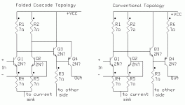
How about a folded cascode to replace the VAS & cascode?
If this works out for you, then we are all going to learn from your endeavours.") good luck symming and listening.
good luck symming and listening.
have you tried sym on local feedback cap from cascode emitter to inverting tr base? instead of VAS base.
Then try with and without cascode.
How about a folded cascode to replace the VAS & cascode?
If this works out for you, then we are all going to learn from your endeavours.
good luck symming and listening.Andrew,
Some results:
* When using local feedback from VAS to the inverting input of the diff pair --> oscillation is even more worse. But when connecting is to the non-inverting input --> oscillation is gone or less worse, dependent on the input voltage. (looks like there is phase invertion with these high frequency's.)
*When I delete the emitter folower after the VAS, the amp is stable, but this gves me higher THD on high output power.
*When I take the feedback signal out of the VAS (only from VAS) --> the amp is much more stable and gives better THD with capacitive loads. But, with resistive loads the THD is better when taking feedback from the outputsignal. So, I should mak a combination of these two.
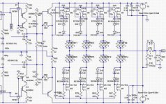
*When I connect a capacitor + resistor (47pF + 68Ohm) from the two outputs of the VAS to ground, the amp is also stabile, but the THS is a bit worser compared to the miller caps. Can you tell me what really the reason is why miller compensation isn't good? See attachment.
Concerning the folded cascode: this I really don't wan't to use, this gives me much more voltage loss over this stage than a cascoded VAS. And according to many threads, a folded cascode is many times even more unstable then a cascoded VAS.
Regards
Ben
Some results:
* When using local feedback from VAS to the inverting input of the diff pair --> oscillation is even more worse. But when connecting is to the non-inverting input --> oscillation is gone or less worse, dependent on the input voltage. (looks like there is phase invertion with these high frequency's.)
*When I delete the emitter folower after the VAS, the amp is stable, but this gves me higher THD on high output power.
*When I take the feedback signal out of the VAS (only from VAS) --> the amp is much more stable and gives better THD with capacitive loads. But, with resistive loads the THD is better when taking feedback from the outputsignal. So, I should mak a combination of these two.
*When I connect a capacitor + resistor (47pF + 68Ohm) from the two outputs of the VAS to ground, the amp is also stabile, but the THS is a bit worser compared to the miller caps. Can you tell me what really the reason is why miller compensation isn't good? See attachment.
Concerning the folded cascode: this I really don't wan't to use, this gives me much more voltage loss over this stage than a cascoded VAS. And according to many threads, a folded cascode is many times even more unstable then a cascoded VAS.
Regards
Ben
Attachments
Don't collect thread opinions, do a correct circuit analysis
Please can you explain why? A folded cascode is a single stage design, gives only 90° max. phaseshift above its corner frequency. As well as a cascoded VAS stage it's an RF design which is sensitive to a bad setup.
Again, why?
And according to many threads, a folded cascode is many times even more unstable then a cascoded VAS.
Please can you explain why? A folded cascode is a single stage design, gives only 90° max. phaseshift above its corner frequency. As well as a cascoded VAS stage it's an RF design which is sensitive to a bad setup.
this I really don't wan't to use, this gives me much more voltage loss over this stage than a cascoded VAS.
Again, why?
Hi Bocka,
Well I must admit, maybe I better do first some sim's before I give opinions. But these words are comming from well known people here in this forum.
Folded cascode:
I've red that this one is more sensitive to a bad setup than a cascoded vas. The bandwith is of a folded one is very big.
Voltage loss: I've attached a picture (see next post). First you have a voltage loss over Q3 (Vce), this signal is then used to drive Q4, the emitter voltage of Q4 is taken after the load resistor R2 from the diff input. The voltage over R2 is in my design already 10Volts.
With the cascode VAS, I have a loss of about 4Volts.
Yes, there will be other design's that are more suitted to use a folded cascode.
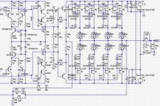
I ran this evening a few hundred sim's, I've been playing with the feedback. I've made a combination of feedback from the VAS and from the output. This results in a pretty good THD amp. When there is a highly capacitive load on the output. You would have enormous amounts of THD in the signal lines wright after the diff pair (pairs). With also the feedback taken from the VAS, the THD stays pretty normal after the diff pair (for example :0.5% VS 25%).
With a input voltage of 1.28VP / 100kHz and load 4Ohm + 1µ, I've a THD of about 0.25%.
With a input voltage of 1.28VP / 1kHz and load 4Ohm + 2µ, I've a THD of about 0.05%.
This is not that bad I guess.
Can anybody tell me whether it is useless to do sim's with these high frequency's to optimalisize the amp, because these are frequency's way out of the audioband. Should I work between 1Hz and 20kHz. And do a check with 100 or 200kHz to see whether the stays stable.
Please, help me out. I have to learn this all from my self, I'v never studied electronics. Just for about 2hours a week at shool.
Greetz
Ben
Well I must admit, maybe I better do first some sim's before I give opinions. But these words are comming from well known people here in this forum.
Folded cascode:
I've red that this one is more sensitive to a bad setup than a cascoded vas. The bandwith is of a folded one is very big.
Voltage loss: I've attached a picture (see next post). First you have a voltage loss over Q3 (Vce), this signal is then used to drive Q4, the emitter voltage of Q4 is taken after the load resistor R2 from the diff input. The voltage over R2 is in my design already 10Volts.
With the cascode VAS, I have a loss of about 4Volts.
Yes, there will be other design's that are more suitted to use a folded cascode.
I ran this evening a few hundred sim's, I've been playing with the feedback. I've made a combination of feedback from the VAS and from the output. This results in a pretty good THD amp. When there is a highly capacitive load on the output. You would have enormous amounts of THD in the signal lines wright after the diff pair (pairs). With also the feedback taken from the VAS, the THD stays pretty normal after the diff pair (for example :0.5% VS 25%).
With a input voltage of 1.28VP / 100kHz and load 4Ohm + 1µ, I've a THD of about 0.25%.
With a input voltage of 1.28VP / 1kHz and load 4Ohm + 2µ, I've a THD of about 0.05%.
This is not that bad I guess.
Can anybody tell me whether it is useless to do sim's with these high frequency's to optimalisize the amp, because these are frequency's way out of the audioband. Should I work between 1Hz and 20kHz. And do a check with 100 or 200kHz to see whether the stays stable.
Please, help me out. I have to learn this all from my self, I'v never studied electronics. Just for about 2hours a week at shool.
Greetz
Ben
Attachments
Bensen said:
Folded cascode:
I've red that this one is more sensitive to a bad setup than a cascoded vas. The bandwith is of a folded one is very big.
Voltage loss: I've attached a picture. First you have a voltage
Attachments
Hi Bensen,
the folded schematic you show should have r2=r1/10 approx.
The voltage at q4 emitter= voltage at q3 base.
Your schematic posted with the two feedback loops is very similar to Leach but with one pole missing. Read Leach again. Borbely also takes a feedback loop from r54/r82 but instead uses diodes for voltage adjustment. Borbely manages his folded without any local feedback cap, although he consistently connects a cap to ground here.
Hi Bensen,
voltage loss of a folded cascode can be reduced to 2-3 volts, very similar to what in a cascoded VAS can be done. In a folded cascode forget about Q3 connect the base of Q4 directly to Q2. R1 can be omitted. Voltage across R2 should be choosen of about 2 volts. To perform this, use two red LEDs to V+ on the base of Q4 for example. Bias through Q2 should be a little bit higher than the sink current Iq of the LTP. So
R2,max = 2V / (2 * Iq)
To prevent oscillation, use a cap of about 100pf from the collector of Q4 to GND. This is a nearly bullet proof solution.
Because the transistor models are too bad (especially for high frequencies) and a sim cannot take parasitaric effects of the real setup into account (i.e. a schematic and this is what a simulation uses, is only a very idealised model of your real circuit)
voltage loss of a folded cascode can be reduced to 2-3 volts, very similar to what in a cascoded VAS can be done. In a folded cascode forget about Q3 connect the base of Q4 directly to Q2. R1 can be omitted. Voltage across R2 should be choosen of about 2 volts. To perform this, use two red LEDs to V+ on the base of Q4 for example. Bias through Q2 should be a little bit higher than the sink current Iq of the LTP. So
R2,max = 2V / (2 * Iq)
To prevent oscillation, use a cap of about 100pf from the collector of Q4 to GND. This is a nearly bullet proof solution.
Can anybody tell me whether it is useless to do sim's with these high frequency's to optimalisize the amp
Because the transistor models are too bad (especially for high frequencies) and a sim cannot take parasitaric effects of the real setup into account (i.e. a schematic and this is what a simulation uses, is only a very idealised model of your real circuit)
Do I always have to set the simulation time so that there is just one period to see? I this one of the rules of sim programs?
You will need an integral (whole) number of cycles to get the best result from the FFT
AndrewT said:
Your schematic posted with the two feedback loops is very similar to Leach but with one pole missing. Read Leach again.
Andrew,
Yes I know, but when I insert a capacitor like Leach, that shortens the feedback from the output to ground on high frequency's, and uses only feedback from VAS. I didn't get good results. THD is the signal lines after the diff pairs is much worser.
Bocka,
Do you mean something like in the attachment? Or do you maybe have a link to a schematic?
I'll give it a go to try a folded cascode this weekend. I will keep you guys updated of my findings.
Greetz
Ben
Attachments
bocka said:Hi Bensen,
voltage loss of a folded cascode can be reduced to 2-3 volts, very similar to what in a cascoded VAS can be done. In a folded cascode forget about Q3 connect the base of Q4 directly to Q2. R1 can be omitted. Voltage across R2 should be choosen of about 2 volts. To perform this, use two red LEDs to V+ on the base of Q4 for example. Bias through Q2 should be a little bit higher than the sink current Iq of the LTP. So
R2,max = 2V / (2 * Iq)
Bocka,
I'm sorry, but I don't know exactly what you mean, I've been trying to draw the schematic like you say. But I can't figure out how to do so.
So, I shouldn't use Q3 as you say. And must connect the base of Q4 to the collector of Q2? What about the emitter of Q4 then? And wy should I use 2 LED's to get 2 volt over R2? With the current source on the diff pair, I can choose R2 that way I have 2volts over it.
Do you maybe have a schematic with this topology or a link or could you maybe draw a sketch?
Greetz
Ben
Andrew,
If you look at the base of the VAS transistor it is hooked up to the drain of one of the differentials, a true folded cascode base is attached to a fixed reference voltage and its drive is applied only to it's emitter.
To answer your question, I believe Curl was first.
Maybe you could call it a partial folded cascode...............
Regards,
Jam
A folded cascode example.
Attachments
jam said:Andrew,
If you look at the base of the VAS transistor it is hooked up to the drain of one of the differentials, a true folded cascode base is attached to a fixed reference voltage and its drive is applied only to it's emitter.
True...

In fact, the second stage is an unbuffered differential stage...
- Status
- This old topic is closed. If you want to reopen this topic, contact a moderator using the "Report Post" button.
- Home
- Amplifiers
- Solid State
- Complementary diff input with JFET and BJT cascode