Hi Bensen,
I might be completely off the wall here, so I am relying on someone correcting me where necessary.
The sym could be spot on and identifying a component combination that eliminates the oscillation.
The sym has drawn your attention to the fact that the circuit is susceptible to component variation.
The slow MJEs are having the same effect as adding damping to the circuit and avoiding the overshoot and repeated corrections that show as oscillation.
So far you have a circuit with ONLY one hi freq compensation, located across the opposite phase LTP load resistors. Well done, no Miller comp caps. But you may need to add some more comp. Try local cap feedback from VAS and/or 2nd LTP stage to inverting input. At least add pads & tracks to your PCB to allow this option if needed at construction. The tracks WILL be very short because all these stages WILL be very close to each other in the final layout. Also add a second feedback resistor location in series with the existing and then add a parallel cap location to this extra resistor. Gives flexibility when debugging.
When setting up the prototype you will need an oscilloscope and thorough testing over a wide range of reactive loads to ensure that oscillation does not occur. A cap load in small increments from 100nF to 2u2F over three voltages 50%, 95% and 105% of maximum input that is just clear of clipping into 4R. If you do square wave testing inject the signal AFTER the RF input filter (not shown at present).
Do a non reactive oscillation test into a load about half the value of your intended speaker load. You should be well inside the SOAR for this test IF you can keep the heatsink cool, i.e. short test periods working quickly or a temporary blower if your measurement and logging are taking a bit longer. A sine wave test signal that is 10 periods ON and 30 periods OFF repeating would substantially reduce your heat loads.
Separate your clean and dirty grounds. You will have three Signal (clean), PCB power (dirty), chassis (safety earth).
Are you adding current limiting Zeners across the gate source pins of the output FETs? If you are, remember to check the current and power dissipation in the drivers when the current limiting is full on.
Finally the 1058/162 have slightly different speeds. The N channel can (should) be slowed down by either increasing the gate resistor or adding a drain gate capacitor to try to match the RC time constant on the FETs, You could try a bit of both.
Nicely put, Andrew T, that about sums it up.
The problem here is that, while 2 early gain stages are good, they and the Vas are more isolated in their pole/zero influences and, while slower Vas BJTs stabilise, they are a C variant substitute for constant C. The difficulty of stabilisation increases with the number of gain stages so - good luck with the CRO and C loads.
Cheers,
Greg
Hi Amp Guru,
I am still a novice at this and learning all the time.
Was your support confirmation that I got it right? i.e. NO errors.
Is the info useful to Bensen? or does my mouth not recognise when to stop talking?
Are there any other tests that should be carried out?
PS my style of learning is trying to understand the message, filtering out the irrelevant/erroneous (the difficult bit), then storing the record. Followed up by implimentation in design and construction.
amplifierguru said:The difficulty of stabilisation increases with the number of gain stages so - good luck with the CRO and C loads.
Cheers,
Greg
Bensen,
this is why I asked you already in post #11, why so many VAS's?
Now you have a new schematic, but still lot of gain stages, don't forget, when the signal reaches the output, it's kind a "too late to fix it" (eg. the distorted signal), with many stages you increase often the propagation delay.
Cheers Michael
AndrewT ,
Thanks for the info, I will try your suggestions. And yes, I actually forgot to play arround with the feedback setup. I have to check the Leach info on the net, about how to design a decent feedback loop.
Good you tell me about the differences of the these two FET's, I will look at other design to see what I can do. I hope to have the Jfet's end of this week, than I will try to build up this amp bit by bit and can do some real live testing. I've red that amps with Jfet input and FET output can sound sometimes harsh. How this comes, I don't know. Haffler and Borbely design's have this also, I never have red anything bad about these amps yet.")
amplifierguru,
Sorry, but I can't make much out of your explanation. My knowledge doesn't yet go so far. But thanks anyway.
Ultima Thule ,
Yes, it looks like there are to much gain stages, but don't forget. In the firste stage I used JFETs --> gain +-4. So I had to use one more extra gain stage, so I used again a diff pair so I could have some error correction again. Amplifierguru believes to have much gain in the error correction, and I'm a believer.
Without the second diff pair, my total gain would be maximum +-6000 with. This looks to less for me.
To me it really look the best option to use both high gain in combination with JFET's. I ran sims in 20 different kind of topology's.
Have you maybe got more knowledge in using Jfet's as input?
I don't really like exotic design's, that is the reason this amp looks pretty straight forward.
Greetz
Ben
Thanks for the info, I will try your suggestions. And yes, I actually forgot to play arround with the feedback setup. I have to check the Leach info on the net, about how to design a decent feedback loop.
Good you tell me about the differences of the these two FET's, I will look at other design to see what I can do. I hope to have the Jfet's end of this week, than I will try to build up this amp bit by bit and can do some real live testing. I've red that amps with Jfet input and FET output can sound sometimes harsh. How this comes, I don't know. Haffler and Borbely design's have this also, I never have red anything bad about these amps yet.
amplifierguru,
Sorry, but I can't make much out of your explanation. My knowledge doesn't yet go so far. But thanks anyway.
Ultima Thule ,
Yes, it looks like there are to much gain stages, but don't forget. In the firste stage I used JFETs --> gain +-4. So I had to use one more extra gain stage, so I used again a diff pair so I could have some error correction again. Amplifierguru believes to have much gain in the error correction, and I'm a believer.
Without the second diff pair, my total gain would be maximum +-6000 with. This looks to less for me.
To me it really look the best option to use both high gain in combination with JFET's. I ran sims in 20 different kind of topology's.
Have you maybe got more knowledge in using Jfet's as input?
I don't really like exotic design's, that is the reason this amp looks pretty straight forward.
Greetz
Ben
Ben,
I'm not too familir with J-FET's, BUT.. I noticed you have S degeneration resistors on them, normaly J-FET's survive quite well witout S resistors as they are still quite linear without them compared to BJT's, remove them and then your gain will jump up, and maybe you don't need a second diff gain stage.
Give it a try..
BTW, if you make a very linear circuit you don't need lot of gain either.
You are also killing lot of gain loading VAS with R4 and R5 if just gain is your goal!
Cheers Michael
My goal isn't gain, but I want to get a pretty normal value +-20000.
I understand wy you would choose to leave the degeneration resistors out, with BJT's this would really help with the gain issue, but with Jfets', the gain is less dependent on the emitter and collector resistor as by BJT's.
The gain when using Jfet's is dependent on IDSS, Vp and also a bit of the load (collector) resistor.
The degeneration resistor by Jfet's is there just to keep the THD low.
I really tryed alot in sim. I don't see any other way that I really like.
R4 and R5 are there to keep the amp a bit more stabel, this is used by elektor in all there amps since 1983. A year before the Crescendo (oscillator) came out. And with these resistors it is pretty easy to calculate the gain also, otherwise it is very dependent on the design after the VAS I think.
Greetz
Ben
Hello again,
I have made the changes to the design. I designed a input filter, a output filter (zobel) and a feedback loop. But the feedback loop can maybe change the way AndrewT proposed, HF feedback from VAS en LF feedback from output with a DCservo.
Can anyone please tell me where to make the split from LF and HF, is this in the 10Hz region, lower or higher?
The frequency response off this amp is:3Hz to 200kHz, these are the -3DB points, those are used wright? Is this a normal response? Looks it wright?
In the SIM I attached a capacitor in parallel with the 4Ohm resistor, but I did'nt get oscillations. I know that SIM are not the same as in reality...
I've split the circuit in two.
Please, tell me your remarqs, that way I can redesign it and make it hopefully better.
Greetz
Ben
Attachments
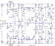
The output circuit:
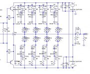
As you can see in my previous post, I've put small capacitors at the N-channel FET's, and I also had to put miller caps at the VAS to stabelize the amp. I don't think 10pF is a big value for this capacitor, but it works really good in the simulation.
Ben
As you can see in my previous post, I've put small capacitors at the N-channel FET's, and I also had to put miller caps at the VAS to stabelize the amp. I don't think 10pF is a big value for this capacitor, but it works really good in the simulation.
Ben
Attachments
Here you can see the Bode-plot:
Looks this alright to you guys?
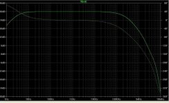
The simulation programm also gives me the THD. This is about 0.4 .. 0.6% dependent on input voltage and frequency. This looks much when compared to regular amps. But I think this is a side effect when using JFET's. With BJT's as input circuit, there would be about 0.01% of THD.
Biasing BTW:
*2.3mA in each leg off the diff amp
*5.7mA in each leg off the second diff amp
*20mA in the VAS section
*I try to get about 35mA, that way I can drive the 4 parallel mosfet's in a decent way.
*+-200mA .. 300mA/MOSFET
Ben
Looks this alright to you guys?
The simulation programm also gives me the THD. This is about 0.4 .. 0.6% dependent on input voltage and frequency. This looks much when compared to regular amps. But I think this is a side effect when using JFET's. With BJT's as input circuit, there would be about 0.01% of THD.
Biasing BTW:
*2.3mA in each leg off the diff amp
*5.7mA in each leg off the second diff amp
*20mA in the VAS section
*I try to get about 35mA, that way I can drive the 4 parallel mosfet's in a decent way.
*+-200mA .. 300mA/MOSFET
Ben
Attachments
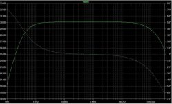
extend your frequency range. some funny things tend to be at >5MHz especially with many coscodes. so far (up to 200kHz) it is ok.
what do these gate caps do?
are you sure they make anything better?
your distortion figures are to high for amount f feedback this high.
check biasing of every stage.
maybe one transistor works close to saturation?
or maybe simulator is aliasing?
keep on!
this can turn out a very good amp!
cheers
what do these gate caps do?
are you sure they make anything better?
your distortion figures are to high for amount f feedback this high.
check biasing of every stage.
maybe one transistor works close to saturation?
or maybe simulator is aliasing?
keep on!
this can turn out a very good amp!
cheers
damn, the more I analyse it the more I get convinced it's gonna be a good amplifier provided you care about all details.
As far harmonic distortion is concerned, I now see that Q1/Q2 work in quite fuzzy application. Try increasing both R20/21 and R4/5, because now Q1/2 VAS needs 14mA (fourteen miliamperes!!!) of AC for full voltage swing.
regards
As far harmonic distortion is concerned, I now see that Q1/Q2 work in quite fuzzy application. Try increasing both R20/21 and R4/5, because now Q1/2 VAS needs 14mA (fourteen miliamperes!!!) of AC for full voltage swing.
regards
Hi darkfenriz ,
I've done the test. I increased the frequency range till 10MHz. But in the SIM, it all seems quite nice to me.
One question, how did you calculate that you need 14mAp-p to get full output swing?
Oh, so you think 0.5%THD is to much for this amp? well I've no experience with JFET's, so I thought this was a normal value. I've red some papers which said that JFET's introduced alot more distorion than BJT's.
I will check the hole amp again in the next couple off days. I can still play around a bit with the values off R20/21 and R4/5. But the value off R4/R20 (R5/R21) may not change alot, otherwise I will lose to much gain.
"what do these gate caps do?"
Well I presume you mean the 10pf caps at the VAS, well without them I have oscillation with a small capaciteve load. I've tryed alot to get rid of this, but when I inserted these caps, I got directly rid off the oscilation.
thanks
Ben
Attachments
One question, how did you calculate that you need 14mAp-p to get full output swing?
well, output of VAS, collectors of Q3/4 "see" 2 parrallel 10k (R4/5) resistors to the ground.
You need swing of 65-70V. So 70V / 5k = 14mA
probably more than idle current in VAS, so you have class AB biasing.
R4/5 should be much bigger.
Oh, so you think 0.5%THD is to much for this amp? well I've no experience with JFET's, so I thought this was a normal value. I've red some papers which said that JFET's introduced alot more distorion than BJT's.
Your 'diamond' differential stage works very good and shouldn't distort so much. You definitely have something wrong if THD is not lower than 0.05%.
sorry for being inprecise, I meant caps on gates of output mosfets.what do these gate caps do?
Are they really needed?
I've done the test. I increased the frequency range till 10MHz. But in the SIM, it all seems quite nice to me.
looks perfect to me
regards
darkfenriz said:
being inprecise, I meant caps on gates of output mosfets.
Are they really needed?
Thanks darkfenriz,
This was a remarq of AndrewT in one of the previous posts. P-channel FET's have much more reverse capacitance than the N-types. 10pF VS 40pF according to the datasheets. To equalise this, I attached these caps. Borbely does just the same when using these output mosfet's.
But I don't see any difference in de SIM, THD and all the rest are staying the same.
I will have a look at the biasing this evening, when I'm back at home from work.
Greetz
Ben
Hi Ben,
the output FET gate caps are in the wrong place. They should be connected from gate to drain (very close to FET output leads). The FET cap values of interest are, I believe, the Cgd of 600pF vs 900pF. I would NOT add the full difference of 300pF, I chose to add just 100pF and increased the gate resistor by 20%.
How hot are the drivers going to run? 50r across the emitters is quite low!
What is the Q2 & Q3 cascode achieving after you have added the Miller comp cap?
Finally you have a Thiel network on the output, not a Zobel.
Hello Andrew,
I thought that the reverse capacity was more important, because this determines whetter there will be cross conduction, am I totaly wrong here? The Borbely amps have the caps at the same place as I have. But I will try to find that out in other threads hopefully. I'm still a novice, I've to learn still many things.
Yes there is about 50Ohm between the drivers, but this can't change alot. I've found this value with" trial and error". The value is dependent on the Bias potentiometer (R19), the resistors R59 and R60, and the bias running throught the MOSFET's. The bias througt the drivers will be around 35mA --> <3W dissipation. This shouldn't be a problem I think.
"What is the Q2 & Q3 cascode achieving after you have added the Miller comp cap?"
Well, I still have the advantages of a cascode. Very less voltage differences over Q2 and Q3 --> less distortion. Without the cascodes, there would be a voltage difference Q2VCE and Q3VCE of about 70V.
Please tell me if I'm totaly wrong here. It looks to me that the miller caps don't do anything to the working off the cascodes.
Again, I learned something new, I didn't know off a Thiel network, I thought that one always used the name Zobel. Thanks. Zobel i probably only the capacitor with the series resistor?
Andrew, do you maybe have any idea what causes this height THD, or does this looks a normal value to you (0.5%).
Greetz
Ben
darkfenriz said:
well, output of VAS, collectors of Q3/4 "see" 2 parrallel 10k (R4/5) resistors to the ground.
You need swing of 65-70V. So 70V / 5k = 14mA
probably more than idle current in VAS, so you have class AB biasing.
R4/5 should be much bigger.
The bias throught this stage is about 19mA.
Hi Ben,
We differ on which capacitance we are trying to match. When your research is productive come back and share your results with us.
Have you plugged the drivers into SOAR yet? Try to estimate the load coming from the output transistors and parallel that with the 50r (or is it half the 50r?). Then plug in the Tc for 3 watts into your chosen heatsink and Rthc-s (it will be HOT unless it shares the main sink) and see what phase angle you can drive. It must be equal to or greater than the output transistor phase angle. MJL1503x can tolerate massive loads & outputs so you will probably be OK, but check it anyway.
re cascode, my limited understanding is that cascode improves the hi freq response and gains in voltage ability in return for susceptibility to oscillation. Your Miller comp cap throws away the hi freq response in bucketloads (worse than BD140 on its own) and you still have all the other complications. So what do you gain? Can an expert on Miller comp and cascode guide us thro' the mire?
Can't help on THD since I have never learned to use a sym. But if that THD were before global feedback you would be in the ballpark but not if it's after applying NFB.
- Status
- This old topic is closed. If you want to reopen this topic, contact a moderator using the "Report Post" button.
- Home
- Amplifiers
- Solid State
- Complementary diff input with JFET and BJT cascode