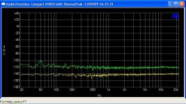
No this is noise floor of the DUT - compact 49810 with thermltrak, though the scale is not dBV.
Odd... What's the dynamic range of the AP?
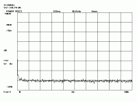
Your measurements show the noise floor at -115ish dB referred to 80 W (25 VRMS). 25 V is +28 dBV. That means the noise floor of the DUT is -87 dBV. I'm measuring -103ish on mine and that's enough noise for me to hear it when I'm close to the speaker.
I don't mean to argue semantics here. I'm just looking for some hard core data to prove me wrong and tell me that I should redesign my board to get rid of ground loops...
")
~Tom
BTW: Pin 3 of the LME49810/11 is marked GND. Which ground is this? In AN-1850 (LME49330 amp), GND is returned to star ground along with the ground from the feedback and power supply decoupling.
I would prefer to have one separate return for supply decoupling, one for feedback, and one for the input. Should the GND pin get its own return to star ground or may it be combined with any of the other?
~Tom
I would prefer to have one separate return for supply decoupling, one for feedback, and one for the input. Should the GND pin get its own return to star ground or may it be combined with any of the other?
~Tom
Odd... What's the dynamic range of the AP?
Your measurements show the noise floor at -115ish dB referred to 80 W (25 VRMS). 25 V is +28 dBV. That means the noise floor of the DUT is -87 dBV. I'm measuring -103ish on mine and that's enough noise for me to hear it when I'm close to the speaker.
I don't mean to argue semantics here. I'm just looking for some hard core data to prove me wrong and tell me that I should redesign my board to get rid of ground loops...
~Tom
Plz note that the 80W there is peak value for a dual-tone 19 + 20 KHz test.
I connect pin 3 to the decoupling ground of the chip, not the input and NFB cap ground.
Noise floor of my AP1 (bottom) and the amp in dBV (AP1 gen off).
I agree with you that 49811 is more sensitive to layout quality.
In my layouts, star grounding is employed. I connect pin 3 to the decoupling ground of the chip, not the input and NFB ground.
Attachments
Last edited:
Panson
Adjusting tempco of diodes is feasible by tuning the bias current of the diode. It can be shown that the tempco ( which is a negative number ) increases ( less negative) with a decrease of bias current. The rule is Delta tempco = 0.2mV/0C per decade decrease of diode current.
The bias pin in the LME49810 is a current source, therefore it is very easy to make a very good bias generator with the TT diodes.
JPV
Thank you JPV. Adjusting the diodes' current is what I am currently doing.
Thank you JPV. Adjusting the diodes' current is what I am currently doing.
Panson,
Let me give you my calculation based on data sheets. My design ( a 10 amps with 4 ways crossover and pic control takes me a lot of time but it is now in final layout stage, hope to make measurements very soon).
You could try this.
My topolgy is a triple Leach as yours but I use the LME49810 which has a pre driver in it. Personnaly I don't see the point to put an external predriver when the guys from National are providing you with a perfectly mached pair pf NPN/PNP. It is a pitty that they provided two diodes to compensate for the Vbe of the predriver. This allows you to use only 4 TT diodes fore the rest of the stages
I use 2 diodes from the output and 2 from the driver ( i am using the same TT as driver).
If you look at the TT datasheet ( 3281/1302) you can find:
Vdiode at 100 microamp = 0.4V and drift of -2mV/°C
Vdiode at 1mA = 0.5V and drift of -1.8mV/°C ( estimated on the curves)
If the current source is 2.45mA then //ing two diodes with 340 ohms will give you 100 microamp in the diodes.
690 ohms will give you 1mA in the diodes.
I use Re's of 0R22 and the Vbe of the output transistor is 0.6V according to the data sheet at that level of current and at 24°C so Vbias required is 4 X 0.6 + 2 x 22mV = 2.452V. This can be tuned in with a potentiometer of 5K set at about 1134 ohms in serie with the 4 TT diodes
Le me know what you think.
BTW: Pin 3 of the LME49810/11 is marked GND. Which ground is this? In AN-1850 (LME49330 amp), GND is returned to star ground along with the ground from the feedback and power supply decoupling.
I would prefer to have one separate return for supply decoupling, one for feedback, and one for the input. Should the GND pin get its own return to star ground or may it be combined with any of the other?
~Tom
Tom,
I will try to think on your layout.
Here are my general thinking about grounding the LME49810 ( purely speculative not based on actual tests).
The ground pin is noisy because it is used for muting logic and clipping logic, return it to output high current ground.
Decouple the LME with power supply with small resistor and electrolytic to high current ground ( these currents may not flow in the sensitive input ground), this is the main PS capacitors point
Bypass with small ceramic very close to the LME, this has to go to input ground.
Put a resistor of a 10 or 100 ohms between ouput and input ground.
Avoid loops of output current generating magnetic field in the input loops.
Take feedback at the output well after the coming together of all the currents.
Zobel output capacitor at the high current return /ground
JPV
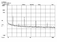
this advice may reduce the buzz showing on your 500Hz plot. I see all mains harmonics from 2nd to 8th about the same level as 60Hz hum. This points to a grounding error..............Decouple the LME with power supply with small resistor and electrolytic to high current ground ( these currents may not flow in the sensitive input ground), this is the main PS capacitors point
Bypass with small ceramic very close to the LME, this has to go to input ground.
Put a resistor of a 10 or 100 ohms between ouput and input ground.
Avoid loops of output current generating magnetic field in the input loops.
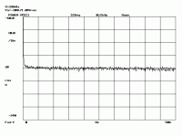
600uVac at the output is bad. +21dB ref 50uVac and -92dB ref 25Vac
I expect <50uVac from all my amplifiers. I have not tested the noise of a 49810, but I have no reason to expect it to be any worse than normal amps.
Tom,
Looking at your shematic I see no major point.
Suggestion:
Remove the servo amp AND its power supply ground to see if this is not the ground loop ( this could star from off board).
Where is the feedback resistor going at the input ( in the connector). It should be tied closely to star input ground to avoid any loop there.
Try to reorient the pc board with respect to transformer to understand if it is magnetic pickup.
Keep us posted, this is interesting
I haven't experienced any severe noise issues with the LME drivers -- but I use a radial system of grounds as Mark recommended in his LM4702 application note. You can not use a ground plane. I've also used a small decoupling resistor on Vcc/Vee of the chip, something like 10 ohms. Mark was also pretty specific about the decoupling caps on the power pins of the device. for economy of space I mounted these on the bottom of the printed circuit boards I had burned.
I believe the reason that these driver chips are "susceptible" to noise is that they stand out there like a high gain radiator (antenna) --
I believe the reason that these driver chips are "susceptible" to noise is that they stand out there like a high gain radiator (antenna) --
Hi JPV,
Thanks for your suggestion.
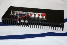
Do you mount the TT driver together with output TT on the main heatsink?
Panson
Thanks for your suggestion.
Do you think 49810 + driver + output better than 49811 + pre-driver + driver + output?My topolgy is a triple Leach as yours but I use the LME49810 which has a pre driver in it. Personnaly I don't see the point to put an external predriver when the guys from National are providing you with a perfectly mached pair pf NPN/PNP.
Do you assume Vbe drift is -2mV/°C?If you look at the TT datasheet ( 3281/1302) you can find:
Vdiode at 100 microamp = 0.4V and drift of -2mV/°C
Vdiode at 1mA = 0.5V and drift of -1.8mV/°C ( estimated on the curves)
If the current source is 2.45mA then //ing two diodes with 340 ohms will give you 100 microamp in the diodes.
690 ohms will give you 1mA in the diodes.
I use Re's of 0R22 and the Vbe of the output transistor is 0.6V according to the data sheet at that level of current and at 24°C so Vbias required is 4 X 0.6 + 2 x 22mV = 2.452V. This can be tuned in with a potentiometer of 5K set at about 1134 ohms in serie with the 4 TT diodes
Le me know what you think.
Do you mount the TT driver together with output TT on the main heatsink?
Panson
Panson,
Yes I assume 2MV/°C drift for the output transistors. I believe this has been measured in another tread.
I mount driver and output on the same heatsink. This is not optimal but I am using a very good forced air cooled heatsink so no problems of pumping there.
The advantage is to mount all the transistors with a pressing profile and belleville washer that keep constant pressure with temperature.
JPV
My issue has ground loop written all over it. See test results below. Improper grounding has been my main suspicion from the start. But I can't for the life of me find that ground loop if there is one... The issue gets further complicated by the fact that I am reusing the chassis of a Parasound A23 that a friend of mine gave me after his girlfriend accidently spilled water in it, thus, killing the amp. I am reusing the input board of the A23 as well as the power supply and heat sink parts. The chassis ground is on the input board. The two amp channels have completely separate power supplies that are grounded to the chassis via the input board. I run the ground of the LME49810 along with the ground for the bypass caps on my driver board to the star ground between the two supply caps. The signal ground is grounded via the shield in the input cable to the input board. I hope this makes sense...
I should probably read that some more...
I bought mine 12-13 years ago from a reputable dealer. I doubt they're fakes. But I have no way of knowing for sure.
Now for the test results and schematics. On the wide-band noise plot, the magenta trace is the amplifier noise floor in dBV with the amp input terminated in 50 ohm, the blue trace is the noise floor of the analyzer (terminated with 50 ohm). The second noise plot shows 0-500 Hz - notice the ripple. This is with the power for the output stage filtered with a pair of 2SC3281/2SA1302 rigged as capacitance multipliers with 1k, 1000 uF on the base. The cap multipliers had negligible impact on the amount of ripple feed-through.
I have these issues on both channels. I have, of course, tried running one channel only and breaking as many grounds in the un-used channel as I could get away with. Still... No dice.
~Tom
Tom, a couple of items:
I suspect either a grounding problem or you cap multiplier isn't doning the job in some way. If you try more bypassing of the chip, it will either eliminate the multiplier as the culprit or implicate it - ie if it get better with more supply bypass, then it's the multiplier, if it doesn't, then it's probably not the problem. Try rigging some good sized caps at the LME board end of your power supply wires min. 4700uf or so.
My on-board supply bypass is comprised of -where the power leads come to the board 100uf || .1uf caps and a .1uf cap between the + & - ;then as close to the power pins of the chip 10uf || .1uf polyproplene caps.
I tried issolating the chip ground from other grounds and it had no measurable effect.
I see that your schematic has seperated the power and signal grounds, I've done the same. I also tied all my signal grounds through a 10 ohm resistor before the star ground. The resistor give a measurable reduction in noise on the signal ground. -You might try this first -
For the time being, I would also take the DC servo out of the circuit so that you can eliminate it as a source of the problem. Just remove the resistors that tie it to the feedback loop. I haven't compared your servo implementation to mine, so, not sure if it's correct or not. I will offef that the LME49720 is not the best choice for a servo op amp. The LF411 / LF412 are much better devices as they have very little DC offset and offset drift with temperature. They are close to perfect for DC servo. The LF411 has to pins that you interconnect with a pot to completely zero out any offset that remains.
Ken
improved DC servo
can you link us to a schematic that shows the trimmer adjustment for zero offset?The LF411 has to pins that you interconnect with a pot to completely zero out any offset that remains.
Andrew,
http://cache.national.com/ds/LF/LF411.pdf
This should work. It's the national data sheet for the chip. First example, first page of the sheet "Typical Connection" the 10k pot between pins 1 and 5 connected to -Vee. The diagram isn't for a DCservo, but the trim is implemented in this configuration within a typical DCservo configuration. I've tried it and it works like a charm.
Ken
Noise floor of my AP1 (bottom) and the amp in dBV (AP1 gen off).
Nice!! Exactly what I was looking for. Thank you very much.
What's the gain of your amp, by the way? The usual THX 29 dB?
In my layouts, star grounding is employed. I connect pin 3 to the decoupling ground of the chip, not the input and NFB ground.
That's what I'm doing as well.
~Tom
@JPV:
As you can see on the schematic, I have local decoupling on the driver board. I'm using 470uF||100nF polyprop for decoupling. This should be adequate for decoupling at audio frequencies. The 100 nF polyprop caps are as close to the LME as practical.
I have tried removing the DC servo op-amp. That doesn't do anything. I have not tried removing its ground, though. That might where the problem lies as I'm sharing the +/-15 V between the two channels. I'll have to track that down.
I forget who asked about the connections to the inverting input of the LME. I'm using this circuit with a differential input, thus, have the amp rigged as a differential amp. The connection to the inverting input of the LME goes to the input XLR connector of the amp.
The cap multiplier is working fine. It reduces 100 mV ripple to 3 mV. But the output of the cap multiplier only feeds the output stage not the LME as I figured the ripple got in via the output stage and would be reduced dramatically by the PSRR of the LME. It was just something I tried as an experiment. Normally, I would feed the output stage directly from the supply. Either way shows the ripple signature I posted last night.
I'm tying the different ground domains together with an RF choke at the star ground. The choke represents about 100 ohm at 100 MHz. I shamelessly ripped this out of the A23 design.
Well... Looking at Panson's data, it's clear that a solid amp can be built with these parts if you get the grounds right. I would have expected nothing less from the National chips anyway. I just need to crack this nut. I'll keep you posted.
Tom
As you can see on the schematic, I have local decoupling on the driver board. I'm using 470uF||100nF polyprop for decoupling. This should be adequate for decoupling at audio frequencies. The 100 nF polyprop caps are as close to the LME as practical.
I have tried removing the DC servo op-amp. That doesn't do anything. I have not tried removing its ground, though. That might where the problem lies as I'm sharing the +/-15 V between the two channels. I'll have to track that down.
I forget who asked about the connections to the inverting input of the LME. I'm using this circuit with a differential input, thus, have the amp rigged as a differential amp. The connection to the inverting input of the LME goes to the input XLR connector of the amp.
I suspect either a grounding problem or you cap multiplier isn't doning the job in some way.
The cap multiplier is working fine. It reduces 100 mV ripple to 3 mV. But the output of the cap multiplier only feeds the output stage not the LME as I figured the ripple got in via the output stage and would be reduced dramatically by the PSRR of the LME. It was just something I tried as an experiment. Normally, I would feed the output stage directly from the supply. Either way shows the ripple signature I posted last night.
I see that your schematic has seperated the power and signal grounds, I've done the same. I also tied all my signal grounds through a 10 ohm resistor before the star ground. The resistor give a measurable reduction in noise on the signal ground.
I'm tying the different ground domains together with an RF choke at the star ground. The choke represents about 100 ohm at 100 MHz. I shamelessly ripped this out of the A23 design.
Well... Looking at Panson's data, it's clear that a solid amp can be built with these parts if you get the grounds right. I would have expected nothing less from the National chips anyway. I just need to crack this nut. I'll keep you posted.
Tom
The plot thickens... I disconnected one channel of the amp and terminated the input to ground via a 10 kOhm resistor. I connected the channel to an HP 6228B lab power supply and made the star ground at the power supply.
The LF noise cleaned up quite a bit, and the even order harmonics of the AC line frequency disappeared. But the odd harmonics (60, 180, 300 ... Hz) are still there. And I still hear a hiss in the speaker with my ear close. The hiss goes away when the amp is muted.
My PCB layout of the amp is definitely not ideal. I could have done a better job with better star grounding, etc. but the layout is not horrible. However, the base connections to the output stage are strung from the right side of the board. So one base connection is approx 20 mm long, the other more like 120 mm... I figured the EF output stage of the LME49810 was low enough impedance to not be bothered by it, but maybe not.
I happen to have a pair of LM3886's. I think I'll play with those a bit on a breadboard and try different grounding techniques on the input. If I can make those ripple free, I should have a chance to get the LME49810's ripple free as well...
Thanks,
~Tom
Attachments
Panson,
I have no idea if 49810 is better or worse than 49811. But if you use a triple topology requiring 2 levels of drivers in class A then It seems to me that having a perfect balanced npn/pnp pair available on chip cannot be beaten by off chip equivalent pair. It simply common sens.
If you uses the 49811 in another topology, then there are pethaps other phenomena.
I made a mistake in my previous post. The resistor required in serie with the diodes is 347 ohms. I am implementing this with a potentiometer and a // 500 ohms resistor. For this, we need the pot at 1134 // with 500 gives 347.
The // 500 ohm is a safety in case the pot fails open circuit, it is in serie with a current source !! and Vbias could go to the roof
JPV
Folks,
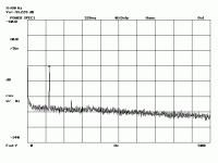
So as promised, here are the noise plots (in dBV/rt(Hz)) for an LM3886 amp with a gain of 20 V/V (26 dB). When building the amp, I made sure to have proper star grounding.
I am fairly certain that the remaining 60 Hz hum is electrostatic coupling into the input and/or feedback. I suppose I could shield the circuit with some aluminum foil to find out for sure, but I haven't bothered.
Initially, I had issues with multiple harmonics of 60 Hz showing up on the output. I got rid of those by grounding the heat sink the LM3886 is mounted to. I'm using the TF version (isolated package).
There's still a very, very faint hiss in the speaker. But the hum is gone. The hiss is only audible when I put my ear 1-2 cm from the tweeter dome so I can live with it.
Bottom line: Star ground does matter.
~Tom
Attachments
- Status
- This old topic is closed. If you want to reopen this topic, contact a moderator using the "Report Post" button.
- Home
- Amplifiers
- Chip Amps
- Comparing LME49810, 49830 and 49811