Hi,
it has been posted here on the Forum that the temperature compensation for the NJLs is not near optimal with 4diodes in series.
It appears that 5diodes in series give somewhere around the correct temp comp.
However, some experiment with diode current is required and the final adjustment will be a series resistor to give the required base to base voltage across the outputs/drivers. There is some evidence that the diode current (slope of temp comp) varies between the various NJLs that ONsemi have released.
The requirement of 5series diodes virtually demands a 3pair output stage.
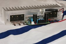
Last days i have built an EF output stage using four pairs of SA1295/SC3264 Sankens driven by (overkill) SA1294/SC3263, SC5i71 as Vbe multiplier all this driven by LME49810.
No self in the output.
I tested with 50v rails for now
20ma cold bias current per device. Very stable after 4 hours working.
I intend to move to 49811, higher rails and triple EF output.
That sounds great.
Very nice chip.
No self in the output.
I tested with 50v rails for now
20ma cold bias current per device. Very stable after 4 hours working.
I intend to move to 49811, higher rails and triple EF output.
That sounds great.
Very nice chip.
Hi,
it has been posted here on the Forum that the temperature compensation for the NJLs is not near optimal with 4diodes in series.
It appears that 5diodes in series give somewhere around the correct temp comp.
However, some experiment with diode current is required and the final adjustment will be a series resistor to give the required base to base voltage across the outputs/drivers. There is some evidence that the diode current (slope of temp comp) varies between the various NJLs that ONsemi have released.
The requirement of 5series diodes virtually demands a 3pair output stage.
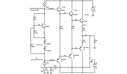
Or you can do this.
D1 and D2 are the Thermal Trak diodes. Adjust R2 and R3 to get correct slope of temp comp. R1 is a pot to adjust bais voltage.
Ken L
Attachments
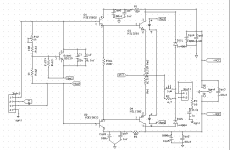
Hi Panson,
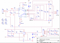
My best results so far. This is using Cordell's bias scheme. I've attached the schematic. I measure the basis with the input signal ground connected, the input open and an 8 ohm load attached. I get 26mv across Re's and 1.226v across the bases of Q3/Q4. I tried running a RMAA test while monitoring the DC voltage across the bases of Q3/Q4 as the signal amplitude went up and down during the test, the voltage declined slightly and then returned within one or two seconds after the amplitude dropped off.
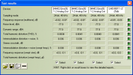
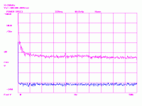
Also attached is the results page. All are measured with an 8 ohm load attached (hopefully I won't make that mistake again) The first three tests from left to right are of the output board as shown in the schematic. They were made in succession each one started soon after the prior finished. The last test is of the LME49811 alone with the source, sink and feed back tied together as shown in the data sheet.
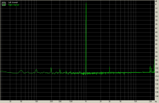
The last image is the THD spectrum from the test on the far left.
Have you looked at the square wave of the LME49811 alone? Mine has some overshoot, not a spike, more of a peaked hump. I tried it with no load and 1k load on the sink and source. Same result.
Ken
My best results so far. This is using Cordell's bias scheme. I've attached the schematic. I measure the basis with the input signal ground connected, the input open and an 8 ohm load attached. I get 26mv across Re's and 1.226v across the bases of Q3/Q4. I tried running a RMAA test while monitoring the DC voltage across the bases of Q3/Q4 as the signal amplitude went up and down during the test, the voltage declined slightly and then returned within one or two seconds after the amplitude dropped off.
Also attached is the results page. All are measured with an 8 ohm load attached (hopefully I won't make that mistake again) The first three tests from left to right are of the output board as shown in the schematic. They were made in succession each one started soon after the prior finished. The last test is of the LME49811 alone with the source, sink and feed back tied together as shown in the data sheet.
The last image is the THD spectrum from the test on the far left.
Have you looked at the square wave of the LME49811 alone? Mine has some overshoot, not a spike, more of a peaked hump. I tried it with no load and 1k load on the sink and source. Same result.
Ken
Attachments
Last edited:
Panson:
I notice that you wire all the ThermalTrack diodes in series in your layouts of the boards with multiple pairs of output devices. Of course, the diodes of the NPN should be in series with those in the PNP, but shouldn't the three pairs of transistors have their diodes in parallel in order to get the correct bias voltage? Or am I missing something?
~Tom
Hi Tom,
The layout has a TT diodes in series. However, any of them can be shorted for fine tuning the thermal compensation circuit.
We can use TT diodes and a trimming pot to form a bias generator. The diode current needs fine tuning to obtain matched Vbe tempco. On the other hand, we can use the TT diodes as part of Vbe multiplier as Leach amp. Numbers of diodes in series for these bias schemes will be different. I am currently working on this interesting issue.
Panson
The response is pretty fast!!!I tried running a RMAA test while monitoring the DC voltage across the bases of Q3/Q4 as the signal amplitude went up and down during the test, the voltage declined slightly and then returned within one or two seconds after the amplitude dropped off.
Ken
Very clean!!!The last image is the THD spectrum from the test on the far left.
Ken
I did not take such a measure for 49811.Have you looked at the square wave of the LME49811 alone? Mine has some overshoot, not a spike, more of a peaked hump. I tried it with no load and 1k load on the sink and source. Same result.
Ken
Panson:
I notice that you wire all the ThermalTrack diodes in series in your layouts of the boards with multiple pairs of output devices. Of course, the diodes of the NPN should be in series with those in the PNP, but shouldn't the three pairs of transistors have their diodes in parallel in order to get the correct bias voltage? Or am I missing something?
~Tom
More thoughts. The four-pair TT layout is a triple-EF output. We therefore have six Vbe. Let's say pre-driver and driver operating temperature are relative stable. We need bias tracking for the output devices, two Vbe. Now we have eight TT diodes from the four pairs. Each diode has a tempco. We may be able to select how many diodes in series to match the tempco of the two Vbe instead of adjusting their current. Or doing both.
Vbias = N x Vd + Vpot (bias voltage generation)
dVbias/dC = N x dVd/dC match with 2 dVbe/dC (bias vs temp change)
adjust N and Id (tuning)
Vbe tempco of TT is not a constant. It also depends on Ib as diode tempco dependence on Id. Ib dynamically changes with source signal. Therefore, tempco of Vbe is varying as well. The about constant tempco is just a simplification.
Any comments?
Last edited:
More thoughts. The four-pair TT layout is a triple-EF output.
That would explain the need for many, many diodes in series...
Vbe tempco of TT is not a constant. It also depends on Ib as diode tempco dependence on Id. Ib dynamically changes with source signal. Therefore, tempco of Vbe is varying as well. The about constant tempco is just a simplification.
Any comments?
I would not expect the tempco of any diode to be completely constant. The voltage drop across the diode will depend on the forward current through the diode to a slight extent, but mostly on temperature. In semiconductor manufacturing, diodes are typically made by shorting the C-B junction of a bipolar transistor or the D-G of a MOSFET. In case of the TT, I would expect the power BJT to be a whole bunch of smaller transistors in parallel. The TT "diode" would then be one of those smaller transistors coupled as a diode. Thus, it's Vd should track the Vbe of the transistor quite well. The matching between the Vbe and Vd is really what counts here - not the absolute tempco.
Have you measured the noise floor of one of your completed amps? I would be very interested in seeing your results. Specifically, LME49810 vs LME49811 with a TT output stage if you have it...
I'm currently using an LME49810 with MJE340/350 drivers and Toshiba 2SA1302/2SC3281 outputs. It sounds OK, but I'm forced to use 66 pF of compensation cap (a real killer on slew rate) and the noise floor is rather high. I forget the numbers, but it's high enough that I hear it up close to my 87 dB/W*m speakers. I haven't had too much time to poke around in it, but I think I'm battling some local oscillation in the driver stage. I also managed to get myself in trouble with some of the routing so I'm thinking to redesign the amp using the TT devices.
~Tom
that sounds more like a wiring error.Have you measured the noise floor of one of your completed amps?................
..........and the noise floor is rather high. I forget the numbers, but it's high enough that I hear it up close to my 87 dB/W*m speakers.
Have you measured the output with a DMM set to 200.0mVac and the input shorted?
That is not the case for TT. The diode characteristic is not the same as the BJT. Please visit Bob Cordell thread on TT http://www.diyaudio.com/forums/soli...al-compensation-thermal-trak-transistors.htmlThat would explain the need for many, many diodes in series...
I would not expect the tempco of any diode to be completely constant. The voltage drop across the diode will depend on the forward current through the diode to a slight extent, but mostly on temperature. In semiconductor manufacturing, diodes are typically made by shorting the C-B junction of a bipolar transistor or the D-G of a MOSFET. In case of the TT, I would expect the power BJT to be a whole bunch of smaller transistors in parallel. The TT "diode" would then be one of those smaller transistors coupled as a diode. Thus, it's Vd should track the Vbe of the transistor quite well. The matching between the Vbe and Vd is really what counts here - not the absolute tempco.
Have you measured the noise floor of one of your completed amps? I would be very interested in seeing your results. Specifically, LME49810 vs LME49811 with a TT output stage if you have it...
I'm currently using an LME49810 with MJE340/350 drivers and Toshiba 2SA1302/2SC3281 outputs. It sounds OK, but I'm forced to use 66 pF of compensation cap (a real killer on slew rate) and the noise floor is rather high. I forget the numbers, but it's high enough that I hear it up close to my 87 dB/W*m speakers. I haven't had too much time to poke around in it, but I think I'm battling some local oscillation in the driver stage. I also managed to get myself in trouble with some of the routing so I'm thinking to redesign the amp using the TT devices.
~Tom
I don't have any oscillation problem with the current Cc = 12 pF. The noise floor can be observed by the FFT here http://www.diyaudio.com/forums/chip...me49810-11-thermaltrak-amp-3.html#post1992585
Panson
It is of course correct that Vbe is changing with Ib but it is not the right approach.
What matter is the distortion at low level ( around the operating point for class AB). This is where the change from first V vs Ic quadrant to the third departs from linearity. For large signals, the emitter follower is linear ( up to a certain level) by its own operation wich involves 100% voltage feedback.
To minimize crossover distortion, there is a theoretical bias current that will generate minimum distortion at that low level of signal when it crosses zero. So total current at higher signal is not related to crossover distortion.
It is therefore important to keep this operating condition constant when the signal crosses zero even if the transistor is hot due to past activity. It is the purpose of the Vbe controller with respect to distortion.. Vbe control is also there of course to avoid thermal runaway.
It can be shown that optimal operating point happens when the bias current in the output transistor is such that : gm Re = 1 where Re is the small emitter resistor. In other words when Ic Re = Vt where Vt is the thermal voltage.
Keeping this Ic operating point constant with temperature is the objective. It is achieved if the Vd diode drift is tracking the Vbe drift with temperature.
The thermal track diode is not part of the transistor silicone it is another diode glued on a common metal frame. This is why the tempco is different. It is anyway faster than a Vbe transistor sensing the heatsink.
Adjusting tempco of diodes is feasible by tuning the bias current of the diode. It can be shown that the tempco ( which is a negative number ) increases ( less negative) with a decrease of bias current. The rule is Delta tempco = 0.2mV/0C per decade decrease of diode current.
The bias pin in the LME49810 is a current source, therefore it is very easy to make a very good bias generator with the TT diodes.
JPV
that sounds more like a wiring error.
Have you measured the output with a DMM set to 200.0mVac and the input shorted?
I have measured with the input terminated by a 50-ohm terminator. I'm getting about 600 uV(RMS) when measuring with an AC voltmeter (BW in the 100's of kHz).
Another thing I've noticed is that it takes FOREVER for the Ve(NPN)-Ve(PNP) to drop after a load transient. By "forever" I mean 45-60 minutes!
One thing I've done that may not have been as clever as I thought is to mount the LME49810 on the same heat sink as the power devices.
~Tom
That is not the case for TT. The diode characteristic is not the same as the BJT.
That's rather lame. It seems to defeat the whole purpose of having a built-in diode... Oh, well... Thanks for the link to the Cordell thread. I'll dig into that.
I don't have any oscillation problem with the current Cc = 12 pF. The noise floor can be observed by the FFT here http://www.diyaudio.com/forums/chip...me49810-11-thermaltrak-amp-3.html#post1992585
12 pF... I must have done something wrong then. I started out with 15 pF (I think it was) and worked my way up to 66 pF before I got rid of some severe peaking in the frequency response. I should go back and revisit.
The noise floor in above plot is actually that of your AP system 1. The reference is 80 W into 8 ohms (0 dB = 25 VRMS). What I'm after is the noise floor with no input signal and 0 dB = 1 VRMS. Units in V/rt(Hz) if possible, but plain dBV would be just as meaningful.
I have an AP script that will convert from dBV to V/rt(Hz) if you're interested. I got it via my local AP distributor/rep. Just let me know if I should dig it out for you.
~Tom
tomchr,
It seems you are not having a particularly good experience with this chip. Some of the published data and personal input by audioman54 and others state that this chip is VERY quiet, more so than many extraordinary discrete amps.
Please continue to provide updates. Much might be learned here.
Tad
It seems you are not having a particularly good experience with this chip. Some of the published data and personal input by audioman54 and others state that this chip is VERY quiet, more so than many extraordinary discrete amps.
Please continue to provide updates. Much might be learned here.
Tad
tomchr,
It seems you are not having a particularly good experience with this chip. Some of the published data and personal input by audioman54 and others state that this chip is VERY quiet, more so than many extraordinary discrete amps.
Please continue to provide updates. Much might be learned here.
Tad
I was indeed a bit surprised to find myself in this kind of hot water as I'm following an NSC app note and have quite a bit of experience both with amplifier design and semiconductor circuit design. I think I need to go back and look at the layout to make sure that everything is connected correctly. Once I'm certain I have no wiring errors, I'll post the schematic and noise measurements.
~Tom
Tom,
In some of my first attempts with the LME49811 I had two issues:
1. It's very sensetive to grounding configuration. Somewhere in the application notes they are quite explicit about grounding schemes. Keeping the signal ground seperate from the voltage ground on the board only connecting them off board at a star ground and the star ground should not be at the power supply capacitors. They mention that in their sample boards, they don't have the speaker ground on the board, to basically force the user to ground the speaker terminal at the star ground as well.
2. I had no luck with Toshiba driver tansistors, odd occillations, other weird stuff. I bought them from a reputable supplier, not ebay. But, I believe that they were fakes... swapped them out for On Semi and the amp runs great. Try a pair of the MJL3281/1302 as your output transistors before you try much else.
Good luck.
Ken
In some of my first attempts with the LME49811 I had two issues:
1. It's very sensetive to grounding configuration.
My issue has ground loop written all over it. See test results below. Improper grounding has been my main suspicion from the start. But I can't for the life of me find that ground loop if there is one... The issue gets further complicated by the fact that I am reusing the chassis of a Parasound A23 that a friend of mine gave me after his girlfriend accidently spilled water in it, thus, killing the amp. I am reusing the input board of the A23 as well as the power supply and heat sink parts. The chassis ground is on the input board. The two amp channels have completely separate power supplies that are grounded to the chassis via the input board. I run the ground of the LME49810 along with the ground for the bypass caps on my driver board to the star ground between the two supply caps. The signal ground is grounded via the shield in the input cable to the input board. I hope this makes sense...
Somewhere in the application notes they are quite explicit about grounding schemes.
I should probably read that some more...
2. I had no luck with Toshiba driver tansistors, odd occillations, other weird stuff. I bought them from a reputable supplier, not ebay. But, I believe that they were fakes...
I bought mine 12-13 years ago from a reputable dealer. I doubt they're fakes. But I have no way of knowing for sure.
Now for the test results and schematics. On the wide-band noise plot, the magenta trace is the amplifier noise floor in dBV with the amp input terminated in 50 ohm, the blue trace is the noise floor of the analyzer (terminated with 50 ohm). The second noise plot shows 0-500 Hz - notice the ripple. This is with the power for the output stage filtered with a pair of 2SC3281/2SA1302 rigged as capacitance multipliers with 1k, 1000 uF on the base. The cap multipliers had negligible impact on the amount of ripple feed-through.
I have these issues on both channels. I have, of course, tried running one channel only and breaking as many grounds in the un-used channel as I could get away with. Still... No dice.
~Tom
Attachments
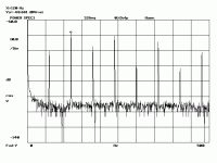
Oh... Ripple. I have about 100 mVRMS of ripple on the supplies for the LME49810. The supplies for the output stage has had its ripple reduced to 3 mVRMS by the cap multiplier.
One channel has slightly higher ripple than the other due to a difference in the bias current in the output stage. The channel with the highest ripple shows the highest ripple components on the output.
~Tom
One channel has slightly higher ripple than the other due to a difference in the bias current in the output stage. The channel with the highest ripple shows the highest ripple components on the output.
~Tom
The noise floor in above plot is actually that of your AP system 1. The reference is 80 W into 8 ohms (0 dB = 25 VRMS). What I'm after is the noise floor with no input signal and 0 dB = 1 VRMS. Units in V/rt(Hz) if possible, but plain dBV would be just as meaningful.
~Tom
No this is noise floor of the DUT - compact 49810 with thermltrak, though the scale is not dBV.
- Status
- This old topic is closed. If you want to reopen this topic, contact a moderator using the "Report Post" button.
- Home
- Amplifiers
- Chip Amps
- Comparing LME49810, 49830 and 49811