You can actually just copy and paste the text for each additional model into the relevant library file (eg bipolars into "standard.bjt") in the LTC directory at:
C:\Program Files\LTC\LTspiceIV\lib\cmp
That way you don't need the .include statement (ie I'm lazy") ). Bob Cordell's models appear with a C suffix so are easily identified when selecting devices.
). Bob Cordell's models appear with a C suffix so are easily identified when selecting devices.
C:\Program Files\LTC\LTspiceIV\lib\cmp
That way you don't need the .include statement (ie I'm lazy
). Bob Cordell's models appear with a C suffix so are easily identified when selecting devices.BTW, why are you running so much current through the VAS? I would think it only needs say 6mA or less, certainly not 40 odd. You're probably just dissipating power for no good reason. Have a look at the currents around the VAS when outputing a 50kHz square wave (as a worst case scenario) and you'll probably find you need much less to slew Cdom adequately. Or perhaps some of the more experienced designers can suggest the best method.
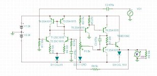
Here's something similar using different parts. The LTP drives an emitter follower which in turn drives an SRPP and a final emitter follower. I don't think there's anything exotic about it. DC offset on the output is -5mV. S/N is 125dB @ 1kHz. Distortion is 6x10^-5% or so for 1.4Vrms output into 10k ohm load. Bandwidth and phase is flat to a GHz or so, then there's a bump. I should probably fine tune the feedback network a little, but I just thought I'd toss another idea out there. The diodes are the CRD (CLD) constant current type. The trim pot is for adjusting the balance of the SRPP.
Attachments
Bandwidth and phase is flat to a GHz or so, then there's a bump.
Are you sure ?
Are you sure ?
All I know is what the software is telling me. Of course, there's no RF filter on the input...
I guess maybe I misspoke. It's early in the morning here. Obviously, it's not flat to a GHz. I meant that there was a bump AT 1GHz or so. sorry.
Attachments
Last edited:
An amplifier of that topology and component values won't work at those frequencies.
I don't know why your simulation program shows such a peak in response at hf. For one thing all the semiconductors are low frequency types (in the scheme of things). 1ghz bandwidth would make a good aerial amp... it's even considered part of the microwave band.
I don't know why your simulation program shows such a peak in response at hf. For one thing all the semiconductors are low frequency types (in the scheme of things). 1ghz bandwidth would make a good aerial amp... it's even considered part of the microwave band.
Hi,
Oli, first memorize Vbe to be roughly 600mV (NPN) or -600mV (PNP). Ony could say that the Emitter of an NPN follows its Base voltage 600mV lower and that the Emitter of a PNP follows its Base voltage 600mV higher.
Then look at Your last schematic again.
The Base of Q6 sits 600mV below the emitter at ~14.4V.
Since Q6 needs only tiny base currents there´s nearly no voltage drop over R6 (its function is to prevent oscillations).
So the node R5/R6/E(Q5) also sits 600mV below the supply voltage at 14.4V. These 600mV divided by the resistance value of R5 defines the current through R5 and into the Emitter of Q5 (base current into Q6 may be neglected here), giving ~6mA.
Now the base of Q5 sits 600mV below its Emitter, hence at 2xVbe below the supply voltage at 13.8V.
Neglecting the low base current of Q7 (hence neglecting voltage drop over R9) the base of Q7 sits at 13.8V and as such its Emitter at 14.4V.
So there´s a voltage drop of 600mV (1xVbe) over R13. With just 10Ohms this calculates to 60mA....way too high. R13 could better be chosen to 100-150Ohms (4-6mA).
Now omit with R2....its of no use here.
The current through R13 and Q7 also flows through D1 and D2, which generates a voltage drop of 2x600mV. The base-emitter path in a transistor functions like a diode, hence the similar voltage drops. So Q8 as well as Q11 open and current flows, but not very defined. If You add a 3rd diode and two Emitter resistors Re8 for Q8 and Re11 for Q11 You can easily calculate the resultant current through Q8 and Q11. Its the third diodes voltage drop divided by the sum of the two resistors. With Re=27Ohms You should end up around 10-15mA. The Diodes need to be thermally coupled with Q8 and Q11. Still though the working point might not be stable over temperature. In that case a ´transistorized Diode´ might be required.
Attached is a ciruit that has been published by Elektor in 1994, the discrete Ulti-Preamp. (I replaced the expensive matched MAT02/MAT03 input transistors with the usual BC550/560)
View attachment discrete Ulti-Preamp.asc
In this schematic the Diodes are replaced by a ´transistorized Diode´ here composed of two transistors (Q9 thermally coupled to Q11, Q10 to Q12), two resistors R18/19 and a linear Poti P1. (Q11/Q12 could be the BD139/140 Pair instead)
jauu
Calvin
An amplifier of that topology and component values won't work at those frequencies.
I don't know why your simulation program shows such a peak in response at hf. For one thing all the semiconductors are low frequency types (in the scheme of things). 1ghz bandwidth would make a good aerial amp... it's even considered part of the microwave band.
Yeah, I agree, so that's why I'm not worried about it.
Hi,
Attached is a ciruit that has been published by Elektor in 1994, the discrete Ulti-Preamp. (I replaced the expensive matched MAT02/MAT03 input transistors with the usual BC550/560)
View attachment 292030
In this schematic the Diodes are replaced by a ´transistorized Diode´ here composed of two transistors (Q9 thermally coupled to Q11, Q10 to Q12), two resistors R18/19 and a linear Poti P1. (Q11/Q12 could be the BD139/140 Pair instead)
jauu
Calvin
That's a very sophisticated circuit! (well, to me anyway) The trim pot didn't show up in my LTSpice. Oh well.
Hi,
well just get rid of Q1,2,6 and throw the damn never really good working dc-servo away, put a decent 1000µ cap between feedback-R30 and gnd and it looks like Olis circuit.
Replace the pot by a fixed resistor value of 25k-27k to vary the output bias current. It is connected as variable resistance anyway.
Oh, btw. if You haven´t recognized it already.....just dragging the "in" label from signal source Vsine to Vsquare changes the sim from sinewave to squarewave. .param Freq=xx changes signal frequency, .param Vin=xx changes signal amplitude.
jauu
Calvin
Sorry, must have had a late night brain fart when I wrote the previous post re VAS current
Looking at the current into Cdom with a HF square wave is useful for checking that the input LTP bias current is adequate for the desired slew rate as it has to charge/discharge Cdom.
To see what sort of VAS bias current is required, load up the output with your expected worst case load (including expected C due to cables and amp input filters - eg 2k2 || 1nF) and have a look at the base current of the output devices. Also bear in mind that the VAS current affects open loop gain so adjusting it might require different values of Cdom for stability. Or you could play with the emitter degeneration of the input LTP instead.
Hi all. Sorry for the late update, I've been busy with work and schoolwork (final year engineering student). Tonight I prototyped the second of the two circuits that Calvin made available in post #11 (the one with the Elektor style compensation). It is excellent! Even on a breadboard there seems to be no high frequency instability at all along with low low noise and high slew rate. I'll take the circuit in with me tomorrow to test on one of the much better oscilloscopes in the lab to double check.
If it checks out, I'll start work on a pcb.
Thanks again Calvin
If it checks out, I'll start work on a pcb.
Thanks again Calvin
So I tested the circuit on a nice Tektronics scope and it appears to be fine. No spikes at the corners of a square wave and a clean waveform - surprising considering it's built on a bread board with little wires going everywhere.
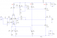
Here's the latest circuit. I figure at this stage that the topology is correct and that it shouldn't be any problem to start drawing a pcb for it.
Can anyone please give me some hints as to how I can work out the optimal component values (assuming they aren't already). I notice in the BC556 data sheet that its optimal collector current is 200uA, however when I tried this, the amp exhibited a little bit of high frequency instability.
Also of interest to me is component type. Specifically for C2, C4 & C13. I've been using NP0 ceramics because I already had some. Will I likely see (or hear) any improvement by exchanging these for film or mica where appropriate?
I have polyprop caps for input and output, polystyrene for decoupling and next month I will aim to get some Nichicon FG caps for C1, C5, C9 & C12 along with some KSA992F transistors for the input, KSC1845 for the VAS and KSA1381 for the output (I'm a poor student so I need to budget for these things) I figure that BC546C will be fine for the current mirror due to high hfe, ditto for the BC556C used in the CCS (please correct me if I am wrong).
Another thing I was curious about is what voltage rating does C5 need? Will it need to be greater than the two supply rails combined?
Attachments
Last edited:
Easy one first. C5 normally sees very little DC voltage such that even a 6.3 volt cap would be OK. It's under fault conditions that it might see significant DC. Also larger working voltage caps tend to perform better so I would suggest a 16 or 25 volt device. Some designers also add an inverse parallel diode across the cap to protect it from reverse bias under fault conditions. It's up to you on that one
C4 at 4.7pf may leave little choice. Ceramic or silver mica. Be aware that a breadboarded layout has loads of stray capacitance and the final PCB version may need this cap altering slightly.
C13 I would use a poly type. Similar for C4. A lot depends on what you can get. Ceramics aren't the best normally when you get to larger values.
Not sure what you are looking at for the 200ua current in the data but I suspect it is a value that some parameters are measured at rather than an optimal value. It's the design of the circuit that dictates what the optimum current may be.
Not familiar with some of those transistors you mention so you will have to look up the data sheets to see they are suitable.
For a design like this any generic NPN/PNP devices will work well such as 2N5551 and 2N5401 etc
Easy one first. C5 normally sees very little DC voltage such that even a 6.3 volt cap would be OK. It's under fault conditions that it might see significant DC. Also larger working voltage caps tend to perform better so I would suggest a 16 or 25 volt device. Some designers also add an inverse parallel diode across the cap to protect it from reverse bias under fault conditions. It's up to you on that one
Thank you. I like the idea of robustness, so I think I'll go with the diode.
C4 at 4.7pf may leave little choice. Ceramic or silver mica. Be aware that a breadboarded layout has loads of stray capacitance and the final PCB version may need this cap altering slightly.
I think I'll use an NP0 ceramic they have a smaller footprint than silvered mica, seem to exhibit good characteristics (from what I've read and observed) and if I need a value that's different from what I already have, they are cheap and readily available.
C13 I would use a poly type. Similar for C4. A lot depends on what you can get. Ceramics aren't the best normally when you get to larger values.
Thanks, it's no trouble to add some little poly caps to my future BOM/shopping list.
Not sure what you are looking at for the 200ua current in the data but I suspect it is a value that some parameters are measured at rather than an optimal value. It's the design of the circuit that dictates what the optimum current may be.
Sorry I should have been a little more specific. The BC556 data sheet quotes its noise figures with a collector current of 200uA. Having read your message and then read the data sheet again, I think you might be right about it just being a value that a parameter was measured at and not an optimal value.
Not familiar with some of those transistors you mention so you will have to look up the data sheets to see they are suitable.
They seem to be suitable but I will research this a little bit further before ordering them. The 2n5551 & 2n5401, also look nice though.
Thanks for all your help, I owe you a beer.
Your welcome, thanks
And good luck with the PCB build. Remember layout is everything. The only other thing to mention is the value of the input and output coupling caps. For the output cap I would probably use 100uf (paralled if you wish with a poly) and add a 100K to ground on the output side (for good practice to terminate the cap to ground)
If it's left floating then the cap could assume some voltage if unconnected and cause pops and bangs when you do connect it to an amp etc.
Edit... I see you have a 47K there which is fine.
The input cap could usefully be a little larger with a 47K input impedance. Say 10uf (and electros aren't all bad).
When the amp is working confirm the polarity of any DC voltage across all these caps to make sure they are fitted the correct way. It's not always obvious depending on offsets... some can go either way so make sure.
And good luck with the PCB build. Remember layout is everything. The only other thing to mention is the value of the input and output coupling caps. For the output cap I would probably use 100uf (paralled if you wish with a poly) and add a 100K to ground on the output side (for good practice to terminate the cap to ground)
If it's left floating then the cap could assume some voltage if unconnected and cause pops and bangs when you do connect it to an amp etc.
Edit... I see you have a 47K there which is fine.
The input cap could usefully be a little larger with a 47K input impedance. Say 10uf (and electros aren't all bad
). When the amp is working confirm the polarity of any DC voltage across all these caps to make sure they are fitted the correct way. It's not always obvious depending on offsets... some can go either way so make sure.
Hi,
congrats to Your working experiment
The optimum bias current depends on frequency range, (source) impedances and ´speed´ aspects and of course transistor characteristics. In general I prefer higher current values. This is good for low source impedance values and ´speed´. The collector current of the input pair has not only to drive base(s) of the following stages, but the associated capacitances. This had been tthe 20pF Miller-cap in the first circuits and now is the collector capacitance of Q10.
This cap needs to charged and discharged, hence a current that increases with frequency. In the latest circuit it also means charging C4. A current mirror load is a good measurement as it allows for double the collector current as maximum charging current, but in the end more current is usually the right way.
There´s a small noise penalty to pay for higher currents, but with highlevel inputs this is usually a parameter of lower importance. In general the lower the source inpedance the higher the required optimal bias current for lowest noise. Besides if You look at the BC55x series transistors datasheets at the parameter of hfe, bandwidth and saturation voltage, You will see that this series has a good current range of ~1-10mA. In this range hfe is nearly constant, bandwidth is high (maximum ~20-30mA, with 200µA BW is much reduced) and saturation voltage remains nearly constant on a low level. So stick with the 1.5mA per input transistor (BC-types, the value could differ with others). Only try to change it if noise is really an issue.
The BCs are fine for this application. They are kind of Workhorses over here for these tasks. You can source them from everybody anywhere and cheap and even as matched pairs.
Zetex/Diodes and Philps/NXP also manufacture matched Duals in SMD casings, which improves the behaviour of difference amps and current mirrors.
I suggest You try matched Dual SMDs for Q1,2 and Q3,4 and maybe also Q5,6. Heat dissipatation of all 3 pairs would be well within the limits.
e.g. Infineon B846S/847S, BC856S/857S, or BC847BS, BC857BS of Zetex/Diodes, or BCM847BS/857BS of Philips/NXP. All in a SOT363 SMD-casing which is quite easy to solder (6 pins, the two transistors arranged such one could flip the device´s orientation 180° -->failsafe).
I´d only choose throughhole for devices with considerable heat dissipation which are Q7,Q8 (~85mW) and more so Q10 and Q11 (~0.75W).
There´s little to nothing speaking against highquality ceramic caps of the COG or NPO type, especially if You use SMD casings. With film caps there are PEN and more so PPS which are well suited.
The F-1/-3dB of the 1µF input cap are 6.6/3.3Hz. With the suggested 2µ2 the -1/-3dB-freqs become 1.5/3Hz. I wouldn´t go larger, since larger caps always mean more stored energy. At the output do as Mooly suggested and add a 100k ballast after the cap. Here You need a larger cap, if the load impedance of the following devive is not fixed or known. For all impedances above 10kOhm the F-3dB stays below 5Hz if the cap is 3µ3 or larger.
C5 doesn´t need to be 1000µ. 100-220µF is totally sufficient and much smaller in size, even SMD possible, since the voltage rating may be low. If You feel unsure about the rating add a diode (1N4148) in parallel to the cap as protective device.
The most difficult are the values of R18 and C4. As I mentioned before I just threw in a set of ´starting´ values and probabely not the optimum. These might need tweaking. But if a 10kHz rectangle still looks perfect if You drive a couple of meters of cable, then I wouldnt change values.
jauu
Calvin
Hi,
congrats to Your working experiment
Thank you!
The optimum bias current depends on frequency range, (source) impedances and ´speed´ aspects and of course transistor characteristics. In general I prefer higher current values. This is good for low source impedance values and ´speed´. The collector current of the input pair has not only to drive base(s) of the following stages, but the associated capacitances. This had been tthe 20pF Miller-cap in the first circuits and now is the collector capacitance of Q10.
This cap needs to charged and discharged, hence a current that increases with frequency. In the latest circuit it also means charging C4. A current mirror load is a good measurement as it allows for double the collector current as maximum charging current, but in the end more current is usually the right way.
There´s a small noise penalty to pay for higher currents, but with highlevel inputs this is usually a parameter of lower importance. In general the lower the source inpedance the higher the required optimal bias current for lowest noise. Besides if You look at the BC55x series transistors datasheets at the parameter of hfe, bandwidth and saturation voltage, You will see that this series has a good current range of ~1-10mA. In this range hfe is nearly constant, bandwidth is high (maximum ~20-30mA, with 200µA BW is much reduced) and saturation voltage remains nearly constant on a low level. So stick with the 1.5mA per input transistor (BC-types, the value could differ with others). Only try to change it if noise is really an issue.
The BCs are fine for this application. They are kind of Workhorses over here for these tasks. You can source them from everybody anywhere and cheap and even as matched pairs.
This info is absolutely golden. I was very confused about the level of current necessary for the input stage until this post. And also thank you for the reassurance regarding BC54x/BC55x transistors, I had, had a fear that using such cheap transistors may come back to bite me - but I guess they can't be very bad considering the test results so far.
I suggest You try matched Dual SMDs for Q1,2 and Q3,4 and maybe also Q5,6. Heat dissipatation of all 3 pairs would be well within the limits.
e.g. Infineon B846S/847S, BC856S/857S, or BC847BS, BC857BS of Zetex/Diodes, or BCM847BS/857BS of Philips/NXP. All in a SOT363 SMD-casing which is quite easy to solder (6 pins, the two transistors arranged such one could flip the device´s orientation 180° -->failsafe).
I´d only choose throughhole for devices with considerable heat dissipation which are Q7,Q8 (~85mW) and more so Q10 and Q11 (~0.75W).
This is a great idea. While I had intended to use smd resistors as I already have some, I was unaware however of matched 8xx series transistors available in a dual package. The BCM8x7 look especially good and are easily sourced so they will definately be used in my final design.
There´s little to nothing speaking against highquality ceramic caps of the COG or NPO type, especially if You use SMD casings. With film caps there are PEN and more so PPS which are well suited.
Excellent. This along with Mooly's comment has reinforced my opinion of NPO/COG capacitors as being perfectly fine for this role.
The F-1/-3dB of the 1µF input cap are 6.6/3.3Hz. With the suggested 2µ2 the -1/-3dB-freqs become 1.5/3Hz. I wouldn´t go larger, since larger caps always mean more stored energy. At the output do as Mooly suggested and add a 100k ballast after the cap. Here You need a larger cap, if the load impedance of the following devive is not fixed or known. For all impedances above 10kOhm the F-3dB stays below 5Hz if the cap is 3µ3 or larger.
C5 doesn´t need to be 1000µ. 100-220µF is totally sufficient and much smaller in size, even SMD possible, since the voltage rating may be low. If You feel unsure about the rating add a diode (1N4148) in parallel to the cap as protective device.
Brilliant suggestions, I will take them all on board.
The most difficult are the values of R18 and C4. As I mentioned before I just threw in a set of ´starting´ values and probabely not the optimum. These might need tweaking. But if a 10kHz rectangle still looks perfect if You drive a couple of meters of cable, then I wouldnt change values.
Tomorrow I should have access again to a better oscilloscope. I'll load up the output with a long cable and see what happens. If anything goes astray I will tweak the values until it looks correct again and report the findings.
Thanks again you guys. I think I've learned more in the past two weeks about discrete amps than I have in years of reading about the subject. The info you've provided has been succinct and easy to understand - perfect for anybody diving head first in to class A preamps.
Hmmm interesting.
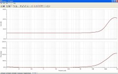
So I managed to get my hands on a decent 1980's vintage, tektronics oscilloscope. I then proceded to follow Calvin's advice for loading up the output with a couple of meters of cable to test for stability. Everything appeared fine, square waves at 10kHz were square. I then decided to check what the wave would look like if there was no feedback compensation cap (C2 from post 34) and I was in for a bit of a shock - lots of high frequency distortion.
So I increased the value of C4 from 1nF to 3nF and it reduced it a little bit. I then tried 8nF and it reduced a little bit more and kept going until I reached 100nF and didn't see any more improvement beyond this point, but by now it was a great deal better than when I started; now just a couple of bumps.
I then re-inserted C2 into the cct as a 4.7pF cap and checked the output (still at the end of a length of coax) and it looked perfect again.
Am I doing it right?
- Status
- This old topic is closed. If you want to reopen this topic, contact a moderator using the "Report Post" button.
- Home
- Source & Line
- Analog Line Level
- Class A preamp: please critique my circuit and give me helpful suggestions.