regarded this topology I started the follow thread for some weeks:Hi all
Other option: buffer + LENDER VAS + buffer
Opinions
http://www.diyaudio.com/forums/soli...age-large-voltage-swings-lenders-circuit.html
and also by this thread you find informations:
http://www.diyaudio.com/forums/solid-state/140461-tgm-amplifier-33.html#post1847644
Last edited:
Hi all
Other option: buffer + LENDER VAS + buffer
Opinions
I do not think you can call your circuit as being a Lender.
See schematics b, at right of the picture :
High perfomance audio power ... - Google Livres
and some comments here :
http://www.diyaudio.com/forums/soli...age-your-zero-feedback-design.html#post436274
I really don't understand the avoidance of current mirror at the diff pair output - automatic balancing of the diff pair is much better than trying to match V+, tail R, collector R to VAS Q (current, temperature variable) ib, Vbe
the potential gain increse helps too
most people also like the increased psrr of a tail ccs
the potential gain increse helps too
most people also like the increased psrr of a tail ccs
I really don't understand the avoidance of current mirror at the diff pair output - automatic balancing of the diff pair is much better than trying to match V+, tail R, collector R to VAS Q (current, temperature variable) ib, Vbe
the potential gain increse helps too
most people also like the increased psrr of a tail ccs
A rumour going round about how it "sounds" bad.

JCX,
Good point. The answer is more in the way humans hear than in the engineering. The two are linked in audio, of course. A little H2/H3 is no bad thing.
If you use a CM, the current through the two degeneration resistors is equal.
BUT, if we ignore the bias requirement of both CM bases from the inactive side (trivial), we are left with the bias requirement for the VAS.
Let us assume both LTP devices are passing 1mA each, 2mA stage current, and the VAS has beta of 150 and runs at 12mA.
Base bias for the VAS is 12/150 = 80uA, and this comes off the 1000uA flowing through the input device of the LTP.
The CM will ensure that of the remaining (920 + 1000)uA which it passes it will be evenly divided, that is, 960uA each. So 960uA goes down the inactive side of the LTP (assuming it's single ended output), but the active input transistor passes 1040uA.
This is not balanced, at least at DC, although it's conceivable that AC might be better balanced. But DC balance is incorrect, and thus operating points are sightly different.
The stock CM is not always the answer, although a Wilson does improve things....
Hugh
JCX,
The CM will ensure that of the remaining (920 + 1000)uA which it passes it will be evenly divided, that is, 960uA each. So 960uA goes down the inactive side of the LTP (assuming it's single ended output), but the active input transistor passes 1040uA.
This is not balanced, at least at DC, although it's conceivable that AC might be better balanced. But DC balance is incorrect, and thus operating points are sightly different.
The stock CM is not always the answer, although a Wilson does improve things....
There is no "inactive" side to the LTP and what you describe IS balanced (<1%), which is at least an order of magnitude better than any thing you'd achieve (especially with temperature) without a current mirror; and especially so in tail current schemes that reference a tail resistor to a supply rail.
And a Wilson current mirror will do nothing for the VAS base current.
with degeneration it is possible to somewhat compensate the VAS base current with the ("feedbacK"?) current mirror
I showed this combination of the JLH mosfet VAS idea and a "balanced" current mirror: (G1,2, I2,3 are a abstract spice model of diff pair)
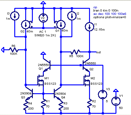
M1,2 equally load both sides of the mirror, R1,2 give equal operating point (still need to coordinate VAS, diff pair CCS to have equal currents in M1,2)
bjt VAS could be done the same - to the degree you can rely on hfe match
even without cascoding - connect the servo Q collector to the amp output and it will have very nearly the same operating point as the VAS Q - maintaining matching over AC operation too
unless monolithic input pair are used I doubt the current density/Shockley Ic/Vbe relation will match to better than 1% when trimmed for 0 V offset, 1% Ic imbalance ~= 0.25 mV input offset
I showed this combination of the JLH mosfet VAS idea and a "balanced" current mirror: (G1,2, I2,3 are a abstract spice model of diff pair)
M1,2 equally load both sides of the mirror, R1,2 give equal operating point (still need to coordinate VAS, diff pair CCS to have equal currents in M1,2)
bjt VAS could be done the same - to the degree you can rely on hfe match
even without cascoding - connect the servo Q collector to the amp output and it will have very nearly the same operating point as the VAS Q - maintaining matching over AC operation too
unless monolithic input pair are used I doubt the current density/Shockley Ic/Vbe relation will match to better than 1% when trimmed for 0 V offset, 1% Ic imbalance ~= 0.25 mV input offset
Last edited:
I would like to agree with Hugh there's not much more balance with a CM loaded diff pair than just resistors, no matter if it's 1% or 0.1% or whatever which is more dependent on the VAS Beta.
And talking about PSRR, well how on earth can a CM loaded diff pair provide that in a typical audio amplifier... remember the audio signal have to swap the reference point from GND to one/or both rails voltages when it goes into the VAS transistor (the VAS transistor is referenced to the rails voltage, right?), how can we escape from that fact...
A resistor at the diff pair output provides a perfect reference, a CM acts as a "black hole" and the GFB system have to take care and correct to make the signal look like referenced to the rails voltage when it's going into the VAS tarnsistor.
And another thing about CM's, have anybody thought about the added Cre (Cob), now not only by the one of the diff transistor but an additional transistor in the CM, the Vbe in the CM is very low typically and we know the Cre grows a lot when Vbe goes down, take that and add it into the equation of the very high impedance of the stage, now how high up is the corner frequency?
Maybe I'm wrong in my assumptions?
Cheers Michael
Last edited:
Precise trim of the diff pair is a 2-d problem – collector area and doping related Vbe differences vary over production but can be pretty good if your lot is all from the same wafer
for minimum distortion you really need to trim with an eye on the distortion output, use a spectrum analyzer – not a multimeter
but maintaining that match is much easier with current mirror load if you expect any Vsupply or tail current variation
nothing prevents you from trimming both Ic ratio and input V offset; Ic ratio with current mirror degeneration resistor ratio trim and Vos with diff pair emitter R trim
the differential Ic currents when subtracted in the current mirror double the gm seen by the VAS – reducing the required diff input error signal by ½ for the same correction “effort”
the distortion of the mirrored diff pair is then less by 2x for any 2nd order remnant and 4x for the 3rd order nonlinear component – the higher n_th order distortion components of the diff pair are reduced by 2^(n-1) factor
the current mirror load is actually also much better in regard to finite and nonlinear output conductance of the diff pair - it differences the two Ic which cancels the common mode portion of the diff pair collector currents whether from input signal or ps movement
a further boost of the psrr can be had with the mirror load, see fig6,7 in:
A General Relationship between Amplifier Parameters and its Application to PSRR Improvement IEEE CAS 1991
more V bias on the mirror transistors is helpful but with discrete amps the bias levels and higher speed of small signal Qs vs the power outputs usually keep mirror pole out of the picture
Last edited:
Member
Joined 2009
Paid Member
Saying "too hard to compensate" or "tends to be unstable"
attracted me to other topologies.
OS
Unfortunately, it works the other way around for me

I like the CFP, but I'm not convinced it provides enough benefit in the VAS.
I tend to agree with others that a single device VAS is hard to beat. But if I went to two devices it would be to make one device a buffer - I like the idea of a buffer before the VAS to provide current drive into Cdom
.....There may be more to be gained by investigating two-pole compensation of the VAS instead of adding extra devices.
Last edited:
Maybe I'm wrong in my assumptions?
Yup.
If you have a single transistor VAS with a resistor "loading" the LTP, the current in that leg (ignoring Ib) is mostly defined by Vbe/R, where Vbe is that of the VAS transistor and R is the resistor.
Vbe changes ~2.2mV per deg C (and a VAS transistor can run rather warm).
If you want the LTP leg currents to be balanced as well as with a current mirror, you need a tail current source that provides exactly double Vbe/R + Ib
that temperature compensates for Vbe - forget about a plain tail resistor here referenced to the opposite supply rail.
Also a CM does not degrade the PSR, if anything it actually improves the rejection WRT noise/ripple on the tail current source. It also dramatically (especially if the VAS is buffered by an EF) raises the loop gain of the VAS, improving VAS linearity and reducing VAS output impedance.
Oh, and the LTP gm is doubled, which gives scope for further linearization of the LTP by means of greater emitter degeneration (while maintaining the same unity loop gain frequency) and the max current delivery to Cdom is approximately double, increasing the slew rate proportionally.
There really is no argument of merit for the technical superiority of a resistively loaded LTP over one with a CM.
Michael,
balance depends on identical properties, the importance of that is a different issue (little, if you asked me). What is important for linearity is to keep Ic stable, which otherwise would constantly vary between zero and max tail current. An increased output impedance improves PSRR, but Cob and voltage gain will also be multiplied by that factor, entailing (in some cases vastly) increased distortion. (The distortion you hear).
balance depends on identical properties, the importance of that is a different issue (little, if you asked me). What is important for linearity is to keep Ic stable, which otherwise would constantly vary between zero and max tail current. An increased output impedance improves PSRR, but Cob and voltage gain will also be multiplied by that factor, entailing (in some cases vastly) increased distortion. (The distortion you hear).
Member
Joined 2009
Paid Member
Gareth,
who`s that beautiful girl? Kinda fiancée?
My avatar ? - no, it's just my taste in girls hair colour
it all started with the movies (5th Element for example)....forget about a plain tail resistor here referenced to the opposite supply rail.
ok, it seems now I missed a bit what the discussion was about as I assumed we had a CCS and not a R tied to our LTP, sorry for that, I do now understand better the point of CM in this discussion. I never talked about what is south of the LTP, on the emitter side, solely the collector side and what follows from there.
I can understand where the CM have some legit benefits in a circuit where the LTP is using a resistor as a current source like DC offset and PSRR.
But this all depends on how the rest of the amplifier is designed which I think you would also agree with.
Many amplifier incorporates a big electrolytic capacitor on the feedback resistor network which makes the amplifier to a unity gain amplifier for a very low frequency and down to DC, other uses DC servo.
"Dramatically raises the loop gain of VAS" I don't really understand, though an EF would have the same benefit for a non-CM LTP input stage driving a typical VAS stage too of course.
"Oh, and the LTP gm is doubled, which gives scope for further linearization of the LTP by means of greater emitter degeneration (while maintaining the same unity loop gain frequency) and the max current delivery to Cdom is approximately double, increasing the slew rate proportionally."
Are you really sure? Have you checked the Cre values for let say a typical small signal BJT like BC550/560? From what I can see checking Fairchilds data sheet the capacitance is not doubled but more than tripled, as I mentioned in my previous post the Cre grows dramatically (on the CM mirror transistor) when Vbc goes down, though not so exponentially as for FET's, and in the case of driving the VAS bjt the Vcb on the CM mirror bjt often stays quite low, that must mean the gain/bandwidth product goes down and thereby also the slew rate, right?
JCX,
thanks for your input as well!
Sure I think it's pretty clear points there and due to me misconstruing the discussion a bit we divided a bit, but I would be very keen to know where do you find the text making the following claims or presentation of data according with your statement:
"the distortion of the mirrored diff pair is then less by 2x for any 2nd order remnant and 4x for the 3rd order nonlinear component – the higher n_th order distortion components of the diff pair are reduced by 2^(n-1) factor"
Unfortunately I don't have access to IEEE.
Cheers Michael
Last edited:
Have you checked the Cre values for let say a typical small signal BJT like BC550/560? From what I can see checking Fairchilds data sheet the capacitance is not doubled but more than tripled, as I mentioned in my previous post the Cre grows dramatically (on the CM mirror transistor) when Vbc goes down, though not so exponentially as for FET's, and in the case of driving the VAS bjt the Vcb on the CM mirror bjt often stays quite low, that must mean the gain/bandwidth product goes down and thereby also the slew rate, right?
Michael,
What do you think the effect of the Ccb of the current mirror transistor is on the GBW, and why? Please state what you believe to be the influence of this Ccb on the GBW (in terms of a simple formula) and how you reached this conclusion.
BTW, if you want that IEEE article jcx references, just shoot me an email. It's about PSRR though, not distortion. And incorporating the PSRR improvement of the article causes some other issues not mentioned in the article, nor in the D. Self book that also covers the PSRR improvement mod.
the distortion math is from the Taylor series expansion of tanh (or any smooth distortion charateristic) under the assumption that the mirror's doubling of the diff pair gm at the VAS input reduces the required signal in the diff pair to ½; the n-1 power instead of n comes from dividing by the signal once to normalize the distortion
Cherry’s “ESTIMATES OF NONLINEAR DISTORTION IN FEEDBACK AMPLIFIERS” JAES V48#4 2000 p299-313
Shows example calculations using just the 2nd and 3rd order distortion terms (I don’t have an electronic copy – for a 1 year AES membership you could download all of the articles)
the mirror transistors can be low voltage RF types - the VAS has to be rated for the full supply V and much larger power so it will have larger Cob and that Cob will be Miller multiplied by the VAS voltage gain of >100 viewed at the input to the VAS so mirror Q Cob is really negligible even before (also Miller multiplied) Cdom is considered
the PSRR paper can be found with Google – I didn’t include a link since CiteSeer had problems earlier today – looked like it might have been a temporary dynamic link
Last edited:
I can understand where the CM have some legit benefits in a circuit where the LTP is using a resistor as a current source like DC offset and PSRR.
But this all depends on how the rest of the amplifier is designed which I think you would also agree with.
Many amplifier incorporates a big electrolytic capacitor on the feedback resistor network which makes the amplifier to a unity gain amplifier for a very low frequency and down to DC, other uses DC servo.
"Dramatically raises the loop gain of VAS" I don't really understand, though an EF would have the same benefit for a non-CM LTP input stage driving a typical VAS stage too of course.
The improved balance LTP balance obtained with a CM actually lowers the input offset voltage.
Regarding the VAS, this stage has local negative feedback provided by Cdom. If the VAS base is tied to the respective rail with a low value resistor the feedback via Cdom is reduced. Add a current mirror and the impedance at the VAS base is increased along with the local feedback provided by Cdom, and the VAS linearity improves. This is (mostly) why an EF buffer for the VAS gives such a dramatic improvment to linearity - it raised the VAS input impedance further.
"Oh, and the LTP gm is doubled, which gives scope for further linearization of the LTP by means of greater emitter degeneration (while maintaining the same unity loop gain frequency) and the max current delivery to Cdom is approximately double, increasing the slew rate proportionally."
Are you really sure? Have you checked the Cre values for let say a typical small signal BJT like BC550/560? From what I can see checking Fairchilds data sheet the capacitance is not doubled but more than tripled, as I mentioned in my previous post the Cre grows dramatically (on the CM mirror transistor) when Vbc goes down, though not so exponentially as for FET's, and in the case of driving the VAS bjt the Vcb on the CM mirror bjt often stays quite low, that must mean the gain/bandwidth product goes down and thereby also the slew rate, right?
Yes I am sure. The reason why the gm of the LTP is effectively doubed when a CM is added is because the current in each leg is utilised to provide push-pull drive to the VAS.
In this kind of topology the maximum possible slew rate is determined by the current that the LTP can deliver to Cdom. With a current mirror on the LTP, this current is doubled.
- Status
- This old topic is closed. If you want to reopen this topic, contact a moderator using the "Report Post" button.
- Home
- Amplifiers
- Solid State
- CFP For The VAS