Constant power diffs can be problematic to control, but with huge linear current gain, they present virtually no load to the input stage.") This one uses dynamic bias with source feedback and miller lag compensation in a balanced bridge configuration. It will take a while to draw out, my only drawing of it disappeared during spring cleaning.
This one uses dynamic bias with source feedback and miller lag compensation in a balanced bridge configuration. It will take a while to draw out, my only drawing of it disappeared during spring cleaning. 
Perhaps when I get back, I have to leave town for a few days.
This one uses dynamic bias with source feedback and miller lag compensation in a balanced bridge configuration. It will take a while to draw out, my only drawing of it disappeared during spring cleaning. Perhaps when I get back, I have to leave town for a few days.
!
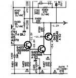
As far I know, boraomega used CFP VAS in Studio amplifier from 1976 year!It's very good amplifer!
Here is schematic
STUDIO SCHEMATIC
As far I know, boraomega used CFP VAS in Studio amplifier from 1976 year!It's very good amplifer!
Here is schematic
STUDIO SCHEMATIC
forr said:
Hi CBS
Well, I was going to ask you to show your best VAS...
I am very interested by constant power schemes.
Hi forr
Sorry for the time delay, I’ve been working out of town trying to not have to live in the streets. Gotta do what you gotta do, eh?
Since I lost my diagram and the computer editing software is being a real pain, I had to sketch it out from memory. Anyway, as you can see this circuit is a balance bridge. Each output, Ch 1 and Ch 2 are intended to drive a HEC hexfet output stage and set the bias spread for each. The output transistor’s +/- Vdd is 24V. Plenty of room with some sag to deliver 40Vp. The outputs are bridged across the speaker. This bridge uses source FB and lag compensation, the caps labeled Cx. Cy is the compensation for the common mode FB loops. As with any circuit, the compensation required for stability is highly influenced by layout. The latest PCB layout I made for this circuit requires all four Cx caps (1-2pf in my circuit) and only one of the Cy caps to get optimum BW and stability. The next layout will be slightly different, but it seems to always take a bit of time to optimize the scheme for each new layout.
I’ve been through about 3 now, , but the latest is the greatest.The transistors labeled 1, 2, 3, 4 are THAT 340 matched arrays. The mosfet gates are at +/- 32V. This is the max voltage output, max swing + the bias spread. This circuit has a rather high FB factor for the balanced mode, with a CL Av of only 4.2. Oooooo…..going to draw fire for that.
 Thus in order to achieve +/- 24Vp swing, it needs +/-5Vp balance input drive. IOW, it needs a pre-amp. For this I used another bridge, but this one is a bit different and uses gate FB with lead compensation. It performs the SE to BAL conversion + gain. Also there are two servos that steer the common mode DC outputs, but they have little to do with CFP. The CL gain of the common mode loop is higher.
 Sort of OP-ampish looking, eh?
Could you imagine trying to match transistor conductance to get perfect balance with such high gain conditions?
Why not mitigate the conductance via the transistor’s source? The outputs bias is quite dependent on the common mode current balance, and the differential mode equalization of it. This whole thing is a culmination of experiments, proving to me that the usual logic for trying to use as few transistors as possible is flawed. Generally this is true, but not necessarily, IMHO.Attachments
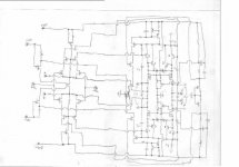
I just remembered the drains of the J-fet's acting as drivers for the cascode BJT to the mosfet gates is actually tied to GND not the collector. The resistor was for power dissipation, but I wanted to maintain a more constant conductance of the J-fet. 40V J-fets are plentiful.
CBS240 said:
I just remembered the drains of the J-fet's acting as drivers for the cascode BJT to the mosfet gates is actually tied to GND not the collector. The resistor was for power dissipation, but I wanted to maintain a more constant conductance of the J-fet. 40V J-fets are plentiful.
Plz have mercy on our eyes, go and get some schematic editor software
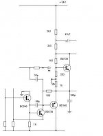
basicly good topology. But I must see the complete circuit, i. e. the (not here to see) input stage and output power stage. Then I can simulate this circuit and I see the consequence of the capacitor values for compensation. This values are depend of many things.
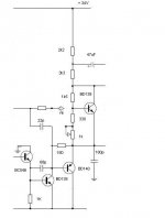
In generall, the idle currents of input and voltage amplifier stages must have values for the max. ft (for small signal types mostly between 4mA and 20mA) The first BD140 (from left) I would replace through such for lower currents (MPS6571, 2N4401).
In generall, the idle currents of input and voltage amplifier stages must have values for the max. ft (for small signal types mostly between 4mA and 20mA) The first BD140 (from left) I would replace through such for lower currents (MPS6571, 2N4401).
Hi All,
Most of the circuits I have seen here in this forum and elsewhere
utilize a single transistor for the VAS. Mr.Self, describing his
'Blameless Amplifier', maintains that it is best to use a darlington
connected pair for the VAS.I would like to hear your opinions
on swapping this darlington configuration with a Sziklai pair.
One downside I can think of is, in a darlington connection as in
Mr. Self's amps, the input transistor of the darlington pair
operates in an almost constant Vce because the collector is
tied to the ground.In a CFP configuration, both transistors
making up the VAS will see the rail-to-rail excursion, forcing
the first transistor to be a high voltage type as well.
Selim
As I note by simulations, there is mainly on advantage by both configutaions:
By the normal darlington I have a little bit lower open loop gain compare to a CFP VAS stage
If I use a CFP (Sziklai Darlington) instead of a normal darlington, the finding of an optimal compensation is more difficult in most cases, because the open loop gain rises. Therefore I prefer the normal darlington configuration for the VAS gain stage (= second gain stage)
The second transistor in the CFP VAS is just an emitter follower. The reason for the better linearity is that the first transistor (the actual VAS) operates with a constant current. This allows the quiescent point to move horizontally on the static characteristic graph instead of crossing the Ic vs Vce lines diagonally. IOW, it stays in a more linear region of operation. If the CFP VAS circuit is then cascode, there is a constant Vce in addition to constant current so the Q-point doesn't really move at all. Since any transistor is not really a linear device (some are better than others in a specific operating range), keeping the Q-point from moving as little as possible will yield the best linear performance.
you don't actually have a CFP VAS in your drawing - without emitter degen there is no feedback
a large improvement comes from just buffering with an ef between the diff pair/mirror and the "VAS" - not true Darlington connection or you get the added Q's Ccb Miller multiplied
cascoding would likely be the next improvement in VAS linearity - although buffering the output, ie more pre-drivers for the output Q can be necessary too to see much improvemnt
the "Baxandall Super Pair" combines the input buffering with output conductance improvement but requires VAS emitter degen
CFP advantages just don't match VAS limitations well - the above steps will improve the VAS more
JLH suggested a small signal Mosfet VAS with bjt cascode - "infinite" current gain and high ouput conductance/low parasitic feedback
Last edited:

buffering the VAS as you say, not Darlington, reduces the change in Ic of the input stage, leading to better linearity of the input stage. Since the input stage is within the fb loop, the amp displays better overall linearity. This is a good thing, no?
JLH suggested a small signal Mosfet VAS with bjt cascode - "infinite" current gain and high ouput conductance/low parasitic feedback
I can agree with this...at 0Hz. But at the bandwidth limit (a few hundred KHz?) this may not be the case.

Last edited:
- Status
- This old topic is closed. If you want to reopen this topic, contact a moderator using the "Report Post" button.
- Home
- Amplifiers
- Solid State
- CFP For The VAS