I would still try to check what we can see with the oscilloscope, connected to the output, as well as what we see on the rails. Make the input AC-coupled and try to sync what you see at 50Hz. Amplitude is going to be rather low - no problem, just set the sensitivity in a way that we can see the waveform.
Come on guys 3 different power supplies has been triedThat would be the best thing to do!
The 1X setting on the probe and the scope come in handy here.

")
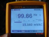
I have trace the rails by scope,if my memory serves well about 10mv ripple
Here is what the millivoltmeter measure on the rails.
Attachments
In any case, seeing the waveforms at the output, at the rails, probably in the star ground on the board may really help to understand the issue.
The thing looks pretty strange right now - the rails are kind of fine, the ground is kind of fine, the spectrum is full of "garbage" from 50Hz to 5KHz. What is it? Let's see the waveform - it may give some ideas
We suppose it's a saw, but... it may be something even more interesting
The thing looks pretty strange right now - the rails are kind of fine, the ground is kind of fine, the spectrum is full of "garbage" from 50Hz to 5KHz. What is it? Let's see the waveform - it may give some ideas
We suppose it's a saw, but... it may be something even more interesting
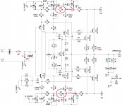
The CFH7/CFH9 amp schematic is very similar to previous CFA/VSSA-type amps as shown in Post 1, so I wonder if those amps also have low PSRR issues? If not then it has to be the layout that is causing this. Perhaps it is a ground loop between the PSU and the input stage?
Thanks for all the debugging Thimios - and sorry it is giving you so much trouble. I wonder if the flying leads on all the actives may be causing some of this?
It may be that the solution is to give this amp the extra PSRR it needs via the cap multiplier, another pair of actives and place it right before the 4700uF cap so that only a small 470uF electrolytic is needed.
The circuit would resemble Idefixes Juma cap multiplier (Cx) blended onto same board. So I see the PCB being elongated to fit one additional pair of IRFP204/9240 for an on-board Cx. It would be called CFH9Cx Then the PSRR is not an issue anymore.
I think Still4given built the CFH7 (Sonal layout) and did not have a hum issue.
Thanks for all the debugging Thimios - and sorry it is giving you so much trouble. I wonder if the flying leads on all the actives may be causing some of this?
It may be that the solution is to give this amp the extra PSRR it needs via the cap multiplier, another pair of actives and place it right before the 4700uF cap so that only a small 470uF electrolytic is needed.
The circuit would resemble Idefixes Juma cap multiplier (Cx) blended onto same board. So I see the PCB being elongated to fit one additional pair of IRFP204/9240 for an on-board Cx. It would be called CFH9Cx
Then the PSRR is not an issue anymore.I think Still4given built the CFH7 (Sonal layout) and did not have a hum issue.
Last edited:
Hi shann,
You should never use the X1 position on a switchable probe. Honestly, I use epoxy and fill that switch actuator with glue. I have had probes switch to X1 before and almost blew a very expensive 'scope up. There is a reason why all good quality oscilloscope probes are X10 only. They do not have a switch.
If you're going to make unattenuated readings, use a normal 50R cable so there is no question as to how it's set. You can buy BNC to alligator clips adapters, and even a premade cable that is BNC to clips.
Be safe and glue those darned switches in the X10 position! At some point you will be extremely glad you did!
-Chris
Valery,i will post soon what you ask about.In any case, seeing the waveforms at the output, at the rails, probably in the star ground on the board may really help to understand the issue.
The thing looks pretty strange right now - the rails are kind of fine, the ground is kind of fine, the spectrum is full of "garbage" from 50Hz to 5KHz. What is it? Let's see the waveform - it may give some ideas
We suppose it's a saw, but... it may be something even more interesting
Have you seen the picture 4 in post #670 where the peeceebee was tested the same time with the same power supply?
X,don't worry may be is mine issue,in any case i don't want another functional amplifier but i want to discover where the bastard are hidden!The CFH7/CFH9 amp schematic is very similar to previous CFA/VSSA-type amps as shown in Post 1, so I wonder if those amps also have low PSRR issues? If not then it has to be the layout that is causing this. Perhaps it is a ground loop between the PSU and the input stage?
Thanks for all the debugging Thimios - and sorry it is giving you so much trouble. I wonder if the flying leads on all the actives may be causing some of this?
It may be that the solution is to give this amp the extra PSRR it needs via the cap multiplier, another pair of actives and place it right before the 4700uF cap so that only a small 470uF electrolytic is needed.
The circuit would resemble Idefixes Juma cap multiplier (Cx) blended onto same board. So I see the PCB being elongated to fit one additional pair of IRFP204/9240 for an on-board Cx. It would be called CFH9Cx
I think Still4given built the CFH7 (Sonal layout) and did not have a hum issue.
Yes,the <<flying>> parts is something bad ,i will try to find a better way.
Thiago,i have try to power vas fron a separate capacitance multiplier without any improvement.I see 2 different things about VSSA.
Current VAS with 36ma is very much increased from 15k to 18k.
R17 and R21 come after the VAS. VAS does not have network RC filter as PEECEEBEE
Last edited:
They are close enough,i see 0v offset in the center of trimmer(offset adj)Hello thimios.
I wonder, are the Input and VAS bjts hFE matched?
The vas transistors are KSA1381E,KSC3503E but not match well.
Last edited:
That could work..................
Temporarily remove the small capacitors in parallel with the 2200uF feedback caps..........
All the electros have paralleled low esr caps. Formula for ringing on the supply rails.
It's the opposite. You need some damping resistance between the capacitors to prevent the inductance creating an unstable 2pole reaction.I always thought small 100nF bypass caps next to large electrolytics were a good idea?
No, it's the inductance combined with the capacitance without adequate resistance that allows the high Q to take over and ring (inadequate phase margin)They can cause ringing due to impedance mismatch?
and this is wrong.95% of amp designs have a 100nF film cap next to power rail caps or feedback caps.
Compare to the advice for opamps:
Use the low esr cap at the power pins and locate the electro a bit further down the supply lines.
It's the extra resistance of the slightly longer traces/wires to the electros that lowers the Q of the 2pole resonance.
Many layout designers are not amplifier designers.
Many here do not recognise that difference in skills.
I see 2 different things about VSSA.
Current VAS with 36ma is very much increased from 15k to 18k.
R17 and R21 come after the VAS. VAS does not have network RC filter as PEECEEBEE
I recently had very good luck converting a JFET (J310) into a CCS by tying G to S and adding limit resistor. It becomes a 2 leg series device that can be placed right where R2 and R3 are. Use J110 should give sufficient current and may help the PSRR?
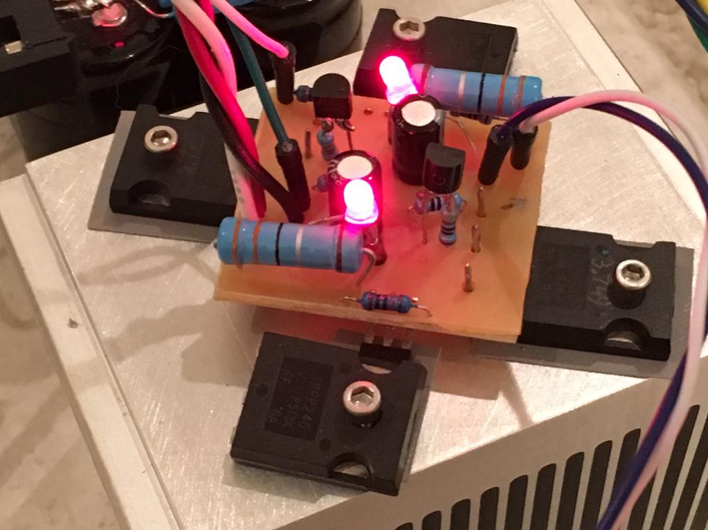
To give you an idea of what that looks like see photo below where TO-92 packages are sitting on top of a vertical resistor. This is my DAO single ended class A head amp.
? are you sure you have described this correctly?I recently had very good luck converting a JFET (J310) into a CCS by tying G to S and adding limit resistor.
you can adjust a jFET CCS to pass less current by adding a resistor to the Source lead out. Then connect this resistor to Gate and this G/R junction becomes the output of the current reduced CCS. Drain remains as the input.It becomes a 2 leg series device that can be placed right where R2 and R3 are..............
Last edited:
? are you sure you have described this correctly?you can adjust a jFET CCS to pass less current by adding a resistor to the Source lead out. Then connect this resistor to Gate and this G/R junction becomes the output of the current reduced CCS. Drain remains as the input.
The J310 has DSG pinouts, I connected pins 2 & 3 together, the current limit is upstream of pin 1 (but suppose it could have been on other side don't know if that makes a difference), the input (+ve side) is pin 1 and output is pins 2&3. Pin 3 was more convenient to use as output pin due to extra spacing between pins but really using pin 2 soldered to pin 3.
http://danssmallpartsandkits.net/J309-D.pdf
So if a J310 has 10mA capability, for this application, we need to calculate what the R value is to get the same current as if R2 was there by itself?
X, CCS topology you describe looks suspicious to me, as well as to AndrewT...
Attached is a good Vishay paper on jFET-based CCS topologies.
jFET has to be negatively-biased, having the current-limiting resistor between the gate and the source.
Having g-s shorted, you have the output current, equal to Idss of the transistor, which is not so good for two reasons - 1) Idss may vary just for manufacturing reasons; 2) It may vary because of non-zero tempco (proper biasing can make it close to zero).
Attachments
Good material on ringing, mentioned above, by Rod Elliott, see 3.1 - Electrolytic Series Resonance:
Capacitor Characteristics
Capacitor Characteristics
Thanks, Valery. I will look into it and perhaps rewire the gate to have resistor in between. I was just throwing together a way to replace an obsolete current source (J511) and probably messed it up. I will try putting the gate so that resistor is in between G and S as you say.
- Home
- Amplifiers
- Solid State
- CFH7 Amp