Peter,
yes, that`s a problem. Maybe more about it later on.
Your speakers need current not high voltages.
Nice parts.
Do you know this site? http://www.dddac.de/op01.htm
yes, that`s a problem. Maybe more about it later on.
Your speakers need current not high voltages.
Nice parts.
Do you know this site? http://www.dddac.de/op01.htm
Attachments
Lumba,
Thank you for your contribution!
I think we share the love for constant current sources!
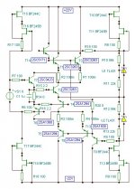
Your schematic is a bit difficult to read (I think you can agree with that") ), but I get the point. This is not a triple but a normal darlington configuration which is much easier to get stable, but will ask more current from the VAS to be driven. Another difference is that the upper part of the cascode is driven from the output instead of the input. That brings me back to my question in post #10. Further is your arrangement is more like the one I posted in post #30, where not the individual stages are cascoded, but the darlington as a whole.
), but I get the point. This is not a triple but a normal darlington configuration which is much easier to get stable, but will ask more current from the VAS to be driven. Another difference is that the upper part of the cascode is driven from the output instead of the input. That brings me back to my question in post #10. Further is your arrangement is more like the one I posted in post #30, where not the individual stages are cascoded, but the darlington as a whole.
Peter
Thank you for your contribution!
I think we share the love for constant current sources!
Your schematic is a bit difficult to read (I think you can agree with that
), but I get the point. This is not a triple but a normal darlington configuration which is much easier to get stable, but will ask more current from the VAS to be driven. Another difference is that the upper part of the cascode is driven from the output instead of the input. That brings me back to my question in post #10. Further is your arrangement is more like the one I posted in post #30, where not the individual stages are cascoded, but the darlington as a whole.Peter
Peter,
Actually, I`d configure the Darlingtons like this for better DC stability.
It is important to always apply clean voltages to bases and gates. Ripple does not sound nice.I think we share the love for constant current sources!
I blame my software.Your schematic is a bit difficult to read
My answer is NO. Vce should be kept constant.That brings me back to my question in post #10 Another difference is that the upper part of the cascode is driven from the output instead of the input.
Well in that case some kind of FET input is to consider.This is not a triple but a normal darlington configuration which is much easier to get stable, but will ask more current from the VAS to be driven.
Actually, I`d configure the Darlingtons like this for better DC stability.
Attachments
Lumba,
Thanks again for your valuable contributions. I have hand drawn your schematic and it looks quite nice!
Perhaps a simulation can give us the answer to what is more accurate in this situation without having to build the circuit.
I am still thinking from a triple darlington perpective (to avoid loading the VAS stage), but perhaps there will be more gain in sound quality by moving over to cascoded output stages than from darlington to triple darlington (which was a clear step up in my case).
At the input there are two current sources to the +/- rails voltages which is very desirable. In ideal situations these are exactly identical. But I have experienced that these can lead to serious DC offset issue’s because in real life two current sources are never the same. It’s hard to get DC offset at the output stable within +/- 100mV (at least for a triple darlington). Do you know a way of avoiding DC offset issues?
The 2SA1360 / 2SC3423 are very nice (low capacitance) devices for VAS stages or at the input of a triple, but not suitable as a driver in a darlington configuration.
Do you have a special reason for double power transistors in the upper part of the cascode and just single power transistors in the lower part?
Peter
Thanks again for your valuable contributions. I have hand drawn your schematic and it looks quite nice!
My answer is NO. Vce should be kept constant.
A few years ago I was working on a tube Cascode stage and measured the how constant the voltage of the lower part of the Cascode was held. It was clear then that the best result were obtained when the upper part got it’s signal from the input.
Perhaps a simulation can give us the answer to what is more accurate in this situation without having to build the circuit.
I am still thinking from a triple darlington perpective (to avoid loading the VAS stage), but perhaps there will be more gain in sound quality by moving over to cascoded output stages than from darlington to triple darlington (which was a clear step up in my case).
At the input there are two current sources to the +/- rails voltages which is very desirable. In ideal situations these are exactly identical. But I have experienced that these can lead to serious DC offset issue’s because in real life two current sources are never the same. It’s hard to get DC offset at the output stable within +/- 100mV (at least for a triple darlington). Do you know a way of avoiding DC offset issues?
The 2SA1360 / 2SC3423 are very nice (low capacitance) devices for VAS stages or at the input of a triple, but not suitable as a driver in a darlington configuration.
Do you have a special reason for double power transistors in the upper part of the cascode and just single power transistors in the lower part?
Peter
Since the two current sources must source and sink the same current, you could use a good pair of current mirrors with carefully matched transistors (or cascoded ones for better accuracy) with common current reference.
I have tried that and it was not good enough. Small temperature changes of the individual transistors of the current mirrors already give too much change in output current, causing DC offset shifts at the output of the amplifier.
Peter
Peter,
By the way, what was the application of that tube stage? For audio frequencies some kind of mu stage is to prefer giving much better load characteristics, distortion figures and driving ability.
Would you please read this post intimating my basic view on things like signal routing.
http://www.diyaudio.com/forums/showthread.php?s=&threadid=118826&perpage=25&pagenumber=1
That parallel has no relevance whatsoever. We are dealing with a solid state output stage here.A few years ago I was working on a tube Cascode stage and measured the how constant the voltage of the lower part of the Cascode was held. It was clear then that the best result were obtained when the upper part got it’s signal from the input.
By the way, what was the application of that tube stage? For audio frequencies some kind of mu stage is to prefer giving much better load characteristics, distortion figures and driving ability.
I doubt it but real life performance can. You are seemingly unwilling to realize the functional difference. You are talking about accuracy I am talking about reducing distortion by holding an important parameter constant.Perhaps a simulation can give us the answer to what is more accurate in this situation without having to build the circuit.
You can still use triple Darlington. Adding a stage however should be justified by clear sonic and/or functional advantages. I am not convinced.I am still thinking from a triple darlington perpective (to avoid loading the VAS stage), but perhaps there will be more gain in sound quality by moving over to cascoded output stages than from darlington to triple darlington (which was a clear step up in my case).
Correct. They are optimized for low current voltage amplification. These devices (video transistors) are so nice that you may easily feel tempted to use them in other places. Types rated 100mA could be chosen.The 2SA1360 / 2SC3423 are very nice (low capacitance) devices for VAS stages or at the input of a triple, but not suitable as a driver in a darlington configuration.
Yes. Current delivery, current and dissipation sharing aiming higher standing current. The upper and the lower part operate very differently.Do you have a special reason for double power transistors in the upper part of the cascode and just single power transistors in the lower part?
Would you please read this post intimating my basic view on things like signal routing.
http://www.diyaudio.com/forums/showthread.php?s=&threadid=118826&perpage=25&pagenumber=1
Yes. DC offset is mainly thermal related, a sure sign of abuse. There are several ways to counteract it depending on the particular situation. More on that later.Do you know a way of avoiding DC offset issues?
pietjers said:This is an update because in the past week I have built and tested the circuit beneath (only with 10V zeners instead of the 5V references).
What most worried me was circuit stability. Well, I must say that these worries have turned out to be true! This circuit is really very hard to get stable. I tried all of the usual ways to get it right (like described in post #59). It is stable under certain circumstances, but during power-up lots of nasty oscillations can be seen that disappear once it’s settled.
Two words:
BASE STOPPERS.
Edit:
Scrap that, I just read post 59.
Even so it didn't fix the instability problem though, high fT BJT double or triple emitter followers quite often won't be oscillation free without base stoppers.
I've done a lot of open loop RF (a few MHz to a few hundred MHz) line driving with discrete emitter / double emitter follower outputs because combined high voltage / high output current / high speed opamps are generally hard to get and expensive.
I've learnt by trial and error that base stoppers are almost mandatory, even to a pair of lowly 2N2219A / 2N2905A EF line drivers.
What most worried me was circuit stability.
Glen,
Sometimes I think it has something to do with me……..

How far (high) can you go with base stoppers?
The drawback is that output impedance rises (I use zero overall feedback) when the value of base stoppers rise (especially at the output devices).
Lumba,
I am working on a way to control the DC offset issue’s. With TL431’s one can make a very simple and super stable (feedback!) CCS’s (see TL431 datasheet). Especially tight when biased with another CCS. The thermal stability is way better than any FET or reference/transistor CCS.
Lumba,
I have a question about the BF244C/BF245B current source in your schematic.
What is the amount of current to expect from this CCS? Is it around 10 mA?
Would be very pleased to hear your thoughts regarding this subject.
Peter
I have a question about the BF244C/BF245B current source in your schematic.
What is the amount of current to expect from this CCS? Is it around 10 mA?
Yes. DC offset is mainly thermal related, a sure sign of abuse. There are several ways to counteract it depending on the particular situation. More on that later.
Would be very pleased to hear your thoughts regarding this subject.
Peter
Hi Peter,
this CCS cascode has very high dynamic impedance and very high bandwidth. The upper FET has to provide sufficient Vds for the lower one, BF244B or C would be fine. We don`t need 10mA here, do we.
R17 sets the current, R1 reduces the voltage (and dissipation) over the FETs leaving, let`s say 5V.
When dealing with JFETs, each one needs to be checked, selected or matched at the intended operating Vds because of a wide variation in their characteristics.
Look, I will answer your questions more precisely but preferably commenting a specific situation, so I would like to know: have you made up your mind about topology and supply voltage?
Lumba,
To be honest, I have built/tested your circuit but I am not able to get it stable. First with a triple lower cascode, and later as a normal darlington configuration, as in your drawing.
So I think I will go back to plain vanilla triple darlington (which is okay) and forget about cascodes for now possibly returning to that subject later when I have finished my current project. For this output stage, which looks very much like the inner part of the circuit posted in post #80, I am looking for a complementary CCS at the input. I have found that with complementary CCS it’s difficult to get stable DC offset performance. My intention is to try a complementary CCS with a LM4041-ADJ in the upper part and a TL431 in the lower part. These devices can be used complementary and have very little temperature drift.
Peter
This what I mean.
Resistor R in the FET CCS must be calculated for a safe voltage drop across the BF244C (what current to expect here?).
Are there ways to avoid DC offset drift besides the use of resistors from the base of the pre-drivers to GND.
Peter
Resistor R in the FET CCS must be calculated for a safe voltage drop across the BF244C (what current to expect here?).
Are there ways to avoid DC offset drift besides the use of resistors from the base of the pre-drivers to GND.
Peter
An externally hosted image should be here but it was not working when we last tested it.
- Status
- This old topic is closed. If you want to reopen this topic, contact a moderator using the "Report Post" button.
- Home
- Amplifiers
- Solid State
- Cascode Output Stages