Professor Leach had one good philia, though, but an expensive one. He documented all the design process for several pieces of common state-of-the-art (for 1970s) audio gear, and later published it online for DIYers. He created a DIYer community sharing designer knowledge. He helped students to build these designs as part of the courses. This is expensive because he had to obtain his earnings from a job as teacher. A professional designer can't publish things like that until the design is well established into the market.
I think it's a generational thing - in the 1960's and '70's transistors were expensive. Double and multi-layer PCBs were also expensive. Simulation software was in it's absolute infancy. Audio gear, while loving to make claims to being high quality, often is high quality only as far as the case - what's inside can be quite crude and ordinary.
Now high-quality multi-layer PCBs are just a few clicks and a few dollars away. Modelling software is pretty damned good, models are pretty good (despite people's claims to the contrary), and transistors are so cheap they're almost free. It's a different way of doing design. I can knock out a design for an amplifier with fifty or sixty active devices in a few days hard work - modelling, schematic and then layout. The tools are just that good.
Gone are the days where designs had to be laboriously worked out on paper before being built - now you can quite reasonably chuck a few parts together and suck it and see - both in the modelling software and with a real live circuit board.
Last edited:
I’ve been building it into things in the last few weeks - a simple 20W (15W woofer and 5W tweeter) active two way speaker, and a slightly over the top stereo (or balanced mono) preamp / headamp (that’s actually capable of putting ~8W into 8 ohms).
Both are coming along nicely, though both will require board respins. The 2 way active speaker pcb went out before I discovered the issue with feedback point, and the preamp first stage has significant H2, possibly because of ground currents issues.
Both are coming along nicely, though both will require board respins. The 2 way active speaker pcb went out before I discovered the issue with feedback point, and the preamp first stage has significant H2, possibly because of ground currents issues.
Hi Suzy,
nice project you start with the noiseunit. Very interesting for making small passive Speakers to an active one.
Following questions:
-is it possible, with the actual equipment of your boards to run these projrct with a transformer 15-0-15 or 18-0-18V AC to achive a litttle more power for bookshelf speakers.
-is it allowed to use your gerbers for ordeing pcb's for privat use, or do sell any pcb's, when debugged the actual one.
- can you give any more information for the calculation over the xover frequencies in the active xover.
- what substitutes can be used for the 2N50XX, since they are hard to find here (any C-types of the BC 54X/55X) series or the SA970 /SC2240BLs)
Happy Easter from Germany and
BR
Günni
Hi Günni,
The +/-18V supply is dictated by the Vceo of the 2N3904/06 of 40V. By substituting MPSA06/56 (80V) or 2N5551/5401 (150V) or another fast, reasonably high gain TO-92 with EBC pinout for all the 2N3904/06, it's possible, in principle, to run the supply higher - say +/-24. Indeed exactly that was in my mind when I added the regulator for the input opamps.
A supply of +/-24V (~18VAC) would allow around +/-20V swing (25W into 8Ω), which should be enough for say 6" mid bass woofers. You'll need to heatsink rather better than I am with the 4" drivers at +/-18V.
No guarantees though - I tried substituting BD139/140 at one stage for the output and had no joy stabilising the amp, so it'd have to be designed and simulated carefully. Indeed I might give it a go - I'll have to buy MPSA06/56's though as I only have about 20 of each in my drawers.
You most certainly have my permission to use the Gerbers for any private or non-profit use.
I'll add detail on the crossover calculations on the noiseUnit page. It's essentially a pair of 4 pole Sallen-Key filters for high & low pass, then a couple of stages of delay for the high pass for time alignment, and a shelf filter for the LF.
Regarding the 2N5087/89, I've actually already ditched these in favour of 2N3904/06. While there's a marginal improvement in simulation using the 2N50XX for the second stage, in practice I see no difference, and the 2N3904/06 are incredibly cheap and plentiful.
There are a couple of other small changes I've made as well - substituting an OPA1652 for one of the OPA1662 opamps to minimise offset at the LF output, tweaking the odd component value etc. I modded the layout as well to fix the issue I was having with feedback point distortion.
I shall update the design files in the noiseUnit thread.
Having played a fair bit with this topology, I reckon I've got a reasonable handle on it's strengths and weaknesses.
Strengths: Reasonably fast, good slew rate, Iq for each output stage implicitly set by diamond source/sink, so no issues with thermal runaway and good at sharing current. Reasonably good distortion performance.
Weaknesses: Maximum current is 2 x Iq x Hfe, so with typical output drivers (BD179/180) with reasonably low Hfe (~40 odd) it's wasting a lot of current for higher wattage flavours.
Also the many cheap output drivers thing, while doable, is rather tedious to build once you include a heatsink, as everything has to be screwed down with individual isolation pads etc, and the expense adds up quickly.
Essentially great for headphones and tweeters, and itty-bitty full range drivers, but not really extendable to bigger things.
So that's led me to look at simpler output stages - essentially returning to a bog-basic emitter follower. I've gotta include a Vbe multiplier, so I inserted it in the middle of the diamond.
The attached sim is a 25W into 8Ω version, using TIP2955 and TIP3055 output drivers set to 20mA Iq, driven by BD139 & BD140 in a diamond. Only the 2955 & 3055 need a heatsink, plus the Vbe multiplier of course. It's really easy to compensate, and makes under 2ppm at 10KHz, with gain set to 6dB. Total amplifier Iq is around 50mA, or 2.4W.
Attachments
Last edited:
but it is exponential not logarithmic. For further enlightenment on semiconductors for ex http://aries.ucsd.edu/NAJMABADI/CLASS/ECE65/12-W/Slides/ECE65_W12-BJT.pdf is recommended. There is no fundamental ic vbe relationship. Cannot be. That is just semiconductor physics.
I'm hoping this is a mistake in language and understanding one another. The very link you shared (I think I ta'd the lab for this exact class a year later) has the vbe ic relationship all over it. I mean, I'll go dig out my device physics books if we want to start from band diagrams.
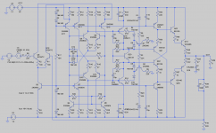
As requested by Chris, here's the stuffing diagrams and BOM for the 10W version. I've used the compensation scheme developed on my noiseUnit woofer driver - this is stable with a gain of 2. It's probably appropriate for a headphone amp - feel free to tweak as you wish.
If you don't want to run small speakers, the output stage current is probably excessive (and needs a heatsink with a power supply >+/-9V or so) - if you substitute 220Ω resistors for R32, 35, 38, 41, 56, 57, 58, 59, 60, 63, 64, 65, 68, 71, 72, and 73 then that will approximately halve the output stage quiescent to 5mA for each of the four sections, and result in 36mW being dissipated by the output transistors with no load at +/-18V supply. It'll drive even low impedance 30Ω cans like this with no heatsink at all.
The doco for the 5W version is further up in the thread.
Attachments
Last edited:
Hi Suzy,
Marvelous! I have both designs saved in directories, printed out and am starting with project boxes.
I have found that putting everything in labeled project boxes (all the same size, and not tiny) allows me to collect the parts without losing anything - including documentation (now stored with the boards). I can also put my hands on any particular project in seconds instead of searching for ever, then hoping I didn't use the parts in something else! A far more sane way to live when you have several projects on the go at once.
I am really looking forward to having these running. Many thanks for your excellent documentation Suzy.
-Chris
Member
Joined 2009
Paid Member
thanks suzyj
Like all amps it depends on the ratio of the feedback resistors. for the 10W version above I was running 6dB (2 x 220Ω). For others I've typically run 20dB (18K & 200Ω).
Thank you suzjj for your deep commitment to this project.
I would like to add my reflection, though I am not an audio designer. This amp has a large open loop gain, around 120 db if I'm not mistaken. We do not know the bandwidth to this gain but I think it is very narrow, at most 1 Khz. This behavior, although it ensures ultra-low distortion in the order of 1 ppm or slightly at higher frequency, such as the last-generation op amps, is not well considered from the point of view of sonic performance. I think it is better to get a distortion of a higher order (10 ppm or less, on the entire audio band seems more than adequate given the much higher distortion of each type of transducer, both speaker or headphone) with a lower open loop gain and a consequent wider open loop bandwidth,(at least 20kHz) that ensures better behavior on the high frequency phase linearity and on the quality of the distortion, at least so it is claim by the people who find the sound of amplifiers so designed very natural and with a very good soundstage.
semola
Hi semola,
 How did you come up with this summary? Did you build one, or have you measured one that is put together?
Actually, if you read the thread you would see that it is a very wide bandwidth circuit. The rest of your statement is just regurgitated audio myth without any basis in fact.
-Chris
We do not know the bandwidth to this gain but I think it is very narrow, at most 1 Khz. This behavior, although it ensures ultra-low distortion in the order of 1 ppm or slightly at higher frequency, such as the last-generation op amps, is not well considered from the point of view of sonic performance.
How did you come up with this summary? Did you build one, or have you measured one that is put together? Actually, if you read the thread you would see that it is a very wide bandwidth circuit. The rest of your statement is just regurgitated audio myth without any basis in fact.
-Chris
It is true that the location of the dominant pole is sometimes called "the open loop bandwidth".
If you take the number called "gain bandwidth product" and divide by the number called "gain" then you get the location of the dominant pole.
Don't get too upset or frosty with somebody who divides "gain bandwidth product" by "gain" and calls the answer "bandwidth". They're not actually wrong, they're just inadvertently abbreviating.
Anatech,
My mistake. Reading more closely the thread, I realized that in the first post the simulations are attached with the data I was looking for. I do not have the software to access the simulation results, so can someone kindly tell me what the open loop bandwidth is? Anyway, my intervention was respectful and I only expressed an opinion based on the data I had at that moment. I do not like the expressions you used to comment on my post, I consider them aggressive and offensive. Although as I wrote, I am not a designer, the idea that a well-sounding project, beyond absolute performance, needs balance between some factors such as gain and open loop bandwidth, adequate slew rate, open loop distortion etc . etc. it does not seem to me a "regurgitating" convictions without foundation, but to cite experiences from many sources based on checks made in the comparison between design parameters and the resulting sound characteristics. Beyond this point I do not push myself because I do not have the technical expertise to support the debate. I wish everyone, and especially suzyj, a useful discussion on a project that seems truly promising and original. Surely I will never make interventions considered "uncalled for", but I wonder what is considered appropriate or not in this forum.....
Greetings
Semola
- Home
- Amplifiers
- Solid State
- Cascading diamond buffers - a cheap low THD 10W amp with TIP41C