Hi John,
looks like the MK6 DAC is almost complete. What is the cost + availability for the DAC module? I have 3x 12V SLA batteries for the PS, can I power the DAC directly from the +12,-12 and -24V rails on the connected batteries?
looking to connect my Squeezebox Duet I2S connections directly to the DAC - please can you advise on a suitable method of taking the clock from the DAC so that I can also try slaving the 11.286 clock on the squeezebox.
I also have one of your SPDIF tracker receivers that I would like to use with the DAC - could I set up the tracker to feed I2S directly into the new DAC, so that I get the full benefit of the new reclocking and attenuation on the MK6?
cheers
Brad
Hi John,
looks like the MK6 DAC is almost complete. What is the cost + availability for the DAC module?.........
I am too very curious to know.
Hi phi,
The bypass resistor values are rather high, approx. 30 M Ohm for a coupling cap, 10K ... 100K for a power supply decoupling cap and approx. 22 K Ohm for speaker crossover filter caps.
The values seem to be too high to effectively dampen high frequency ringing.
I now run my set fully DC-coupled, using a passive adjustable DC bias circuit for each channel. Volume control is passive, based on non-inductive wire wound resistors, and the power amps are also fully DC-coupled.
Coupling caps always add more distortion, noise and coloration compared to a short piece of wire.
The coloration and distortion of a coupling cap can in some cases result in an initial "wow" effect. But after listening for longer time periods, also using different types of music, the "extra" information added by the capacitor can become annoying.
This basically means that every added coupling cap reduces the chance of ever achieving ultimate performance.
If you by 'Charge compensation' mean 'damper', a resistor i parallell with the capacitor that dampens high frequency ringing, then I follow you...
The bypass resistor values are rather high, approx. 30 M Ohm for a coupling cap, 10K ... 100K for a power supply decoupling cap and approx. 22 K Ohm for speaker crossover filter caps.
The values seem to be too high to effectively dampen high frequency ringing.
I now run my set fully DC-coupled, using a passive adjustable DC bias circuit for each channel. Volume control is passive, based on non-inductive wire wound resistors, and the power amps are also fully DC-coupled.
Coupling caps always add more distortion, noise and coloration compared to a short piece of wire.
The coloration and distortion of a coupling cap can in some cases result in an initial "wow" effect. But after listening for longer time periods, also using different types of music, the "extra" information added by the capacitor can become annoying.
This basically means that every added coupling cap reduces the chance of ever achieving ultimate performance.
100 ohm was the value used by the "lampizator" man when a SRPP tube stage followed right after the TDA1541A's output;
and indeed, when I also experimented with his setup 100 ohm was the best value/compromise to use there;
but this stage designed by EC it's a complete different workaround
and indeed, when I also experimented with his setup 100 ohm was the best value/compromise to use there;
but this stage designed by EC it's a complete different workaround
Hi marconi118
TDA1541A output compliance equals +25 / -25mV. Output sinks a constant current from output to -15V that varies between zero and 4mA. It sinks 2mA when no signal is applied (bias current).
When the passive I/V resistor is connected between GND and DAC output a voltage will develop across it as current varies.
The theoretical max. I/V resistor value (I/V resistor tied to GND, so voltage can only go negative) equals R = v / imax. R = 0.025 / 0.004 = 6.25 Ohm. So the indicated value of 100 Ohm is already 16 times too high, distortion will be accordingly. Things can be improved a bit by positioning the ac signal around GND, this requires an additional bias voltage for the passive I/V resistor. However it is extremely difficult to create required ultra low noise reference voltage.
The resulting distortion is caused by the diode transistor bit switches inside the DAC chip that have saturation voltage of approx. 0.6V. The higher the voltage at the DAC output, the more this voltage gets into the non-linear region of the diode characteristic thus causing more distortion until clipping occurs.
I did not connect the passive I/V resistor between DAC output and GND. I connected a grounded-gate buffer between DAC output and passive I/V resistor. The grounded-gate buffer is built around a lateral power MOSFET that basically passes the DAC output current to the passive I/V resistor while maintaining low impedance on the DAC output.
This buffer has low input impedance (approx. 12 Ohms) and high output impedance. There is no output compliance at the buffer output, it could theoretically generate large voltages across a passive I/V resistor. When using 10K I/V resistor (and high enough voltage to feed the I/V resistor) voltage of 0.004 * 10,000 = 40Vpp could be generated while still meeting DAC output compliance.
This offers the unique situation of generating sufficient voltage across a passive I/V resistor without the need for extra amplification or buffering. When using very high performance resistors for passive I/V conversion, noise levels are extremely low, this results in a pitch black background. No tube nor semiconductor output stage could come anywhere close. This configuration also offers highest resolution and lowest sound coloration.
Yes, re-calibration is required when changing I/V resistor value, changing I/V resistor supply voltage or changing DAC chip (tolerances).
Since DC voltage is generated across the passive I/V resistor, 1V when using 500R, varying I/V resistor value will cause large temporary DC shifts on the output. The DC calibration at the DAC outputs also varies as I/V resistor value is varied between o and 100 Ohms. It would also become problematic to get I/V resistor value low enough for achieving very low volume levels.
I use a binary controlled shunt regulator based on high performance non-inductive wire wound resistors for maintaining extreme low noise levels and maximum resolution.
I also applied full DC-coupling using passive adjustable reference voltage for each channel. So the distortion and coloration of the coupling cap is fully eliminated.
In the MK6 the 4mA full scale current will generate 0.004 * 500 = 2Vpp amplitude directly across the passive I/V resistor. The output impedance equals 500 Ohms.
Since I meet TDA1541A output compliance (12 Ohm load), and voltage swing is centered around 0V DC, distortion is close to the values specified in the datasheet.
I have always read that the I/V resistor for TDA1541 should be less than 100Ohm to limit the distortion.
TDA1541A output compliance equals +25 / -25mV. Output sinks a constant current from output to -15V that varies between zero and 4mA. It sinks 2mA when no signal is applied (bias current).
When the passive I/V resistor is connected between GND and DAC output a voltage will develop across it as current varies.
The theoretical max. I/V resistor value (I/V resistor tied to GND, so voltage can only go negative) equals R = v / imax. R = 0.025 / 0.004 = 6.25 Ohm. So the indicated value of 100 Ohm is already 16 times too high, distortion will be accordingly. Things can be improved a bit by positioning the ac signal around GND, this requires an additional bias voltage for the passive I/V resistor. However it is extremely difficult to create required ultra low noise reference voltage.
The resulting distortion is caused by the diode transistor bit switches inside the DAC chip that have saturation voltage of approx. 0.6V. The higher the voltage at the DAC output, the more this voltage gets into the non-linear region of the diode characteristic thus causing more distortion until clipping occurs.
I did not connect the passive I/V resistor between DAC output and GND. I connected a grounded-gate buffer between DAC output and passive I/V resistor. The grounded-gate buffer is built around a lateral power MOSFET that basically passes the DAC output current to the passive I/V resistor while maintaining low impedance on the DAC output.
This buffer has low input impedance (approx. 12 Ohms) and high output impedance. There is no output compliance at the buffer output, it could theoretically generate large voltages across a passive I/V resistor. When using 10K I/V resistor (and high enough voltage to feed the I/V resistor) voltage of 0.004 * 10,000 = 40Vpp could be generated while still meeting DAC output compliance.
This offers the unique situation of generating sufficient voltage across a passive I/V resistor without the need for extra amplification or buffering. When using very high performance resistors for passive I/V conversion, noise levels are extremely low, this results in a pitch black background. No tube nor semiconductor output stage could come anywhere close. This configuration also offers highest resolution and lowest sound coloration.
Changing the I/V resistor value, is it needed to recalibrate the pot on the mosfet gate?
Yes, re-calibration is required when changing I/V resistor value, changing I/V resistor supply voltage or changing DAC chip (tolerances).
is it possible to avoid the volume pot and regulate the volume by changing the 500Ohm I/V value?
Since DC voltage is generated across the passive I/V resistor, 1V when using 500R, varying I/V resistor value will cause large temporary DC shifts on the output. The DC calibration at the DAC outputs also varies as I/V resistor value is varied between o and 100 Ohms. It would also become problematic to get I/V resistor value low enough for achieving very low volume levels.
I use a binary controlled shunt regulator based on high performance non-inductive wire wound resistors for maintaining extreme low noise levels and maximum resolution.
I also applied full DC-coupling using passive adjustable reference voltage for each channel. So the distortion and coloration of the coupling cap is fully eliminated.
In MK6 you use 500Ohm to have higher mV output. Is this leading to distortion?
In the MK6 the 4mA full scale current will generate 0.004 * 500 = 2Vpp amplitude directly across the passive I/V resistor. The output impedance equals 500 Ohms.
Since I meet TDA1541A output compliance (12 Ohm load), and voltage swing is centered around 0V DC, distortion is close to the values specified in the datasheet.
I also applied full DC-coupling using passive adjustable reference voltage for each channel. So the distortion and coloration of the coupling cap is fully eliminated.
Hi EC,
I'm very curious how you got rid of that necessary evil - the coupling cap and it's colorations;
maybe later on you'll be able to show us some simple schematics for us to try your wonderful inovations
Thanks
Hi luxury54,
There is approx. 4V DC on each I/V resistor. So I simply used a 1K potentiometer and suitable decoupling cap to create an adjustable reference voltage. There is a separate reference voltage for L and R channel. This reference voltage now serves as "GND" reference for connected equipment.
By trimming each voltage so it exactly matches DC voltage on the I/V resistor, the DC voltage between I/V resistor and reference becomes zero. In other words, the DC component is removed without using a coupling cap.
The circuit is kept very simple, 1K multiturn trimmer. One side goes to GND, the other to +5V. Suitable decoupling cap is connected between wiper (minus) and +5V (plus). The adjustable reference voltage is now on the wiper.
I tried many semiconductor-based references like buffered bandgap references, diode references, OP-amp based DC servos and so on. As soon as a single semiconductor was used, performance immediately degraded. This was very audible with the double crown chip. I am currently using 1K 15ppm bulk metal foil trimmers and a 470uF/16V Sanyo Oscon decoupling caps.
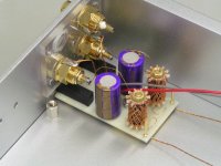
I added a picture of this DC reference module. The two Mobius Honeycomb loops are in the signal path and are used to further purify the signal. This is done by running it through a 2 meter long thin solid-core OFC copper wire. The Honeycomb Mobius structure ensures the piece of wire remains non-inductive and compact. The idea is to improve flow properties of electrical charge.
I'm very curious how you got rid of that necessary evil - the coupling cap and it's colorations;
There is approx. 4V DC on each I/V resistor. So I simply used a 1K potentiometer and suitable decoupling cap to create an adjustable reference voltage. There is a separate reference voltage for L and R channel. This reference voltage now serves as "GND" reference for connected equipment.
By trimming each voltage so it exactly matches DC voltage on the I/V resistor, the DC voltage between I/V resistor and reference becomes zero. In other words, the DC component is removed without using a coupling cap.
The circuit is kept very simple, 1K multiturn trimmer. One side goes to GND, the other to +5V. Suitable decoupling cap is connected between wiper (minus) and +5V (plus). The adjustable reference voltage is now on the wiper.
I tried many semiconductor-based references like buffered bandgap references, diode references, OP-amp based DC servos and so on. As soon as a single semiconductor was used, performance immediately degraded. This was very audible with the double crown chip. I am currently using 1K 15ppm bulk metal foil trimmers and a 470uF/16V Sanyo Oscon decoupling caps.
I added a picture of this DC reference module. The two Mobius Honeycomb loops are in the signal path and are used to further purify the signal. This is done by running it through a 2 meter long thin solid-core OFC copper wire. The Honeycomb Mobius structure ensures the piece of wire remains non-inductive and compact. The idea is to improve flow properties of electrical charge.
Attachments
Hi luxury54,
There is approx. 4V DC on each I/V resistor. So I simply used a 1K potentiometer and suitable decoupling cap to create an adjustable reference voltage. There is a separate reference voltage for L and R channel. This reference voltage now serves as "GND" reference for connected equipment.
By trimming each voltage so it exactly matches DC voltage on the I/V resistor, the DC voltage between I/V resistor and reference becomes zero. In other words, the DC component is removed without using a coupling cap.
The circuit is kept very simple, 1K multiturn trimmer. One side goes to GND, the other to +5V. Suitable decoupling cap is connected between wiper (minus) and +5V (plus). The adjustable reference voltage is now on the wiper.
Hi John,
I once considered such a solution for eliminating the output coupling cap. There are two issues, one minor and one not so minor, that I found.
First, a 'rail-splitting' resistive divider network will substantively increase the circuit output impedance. That's probably a minor concern in a low-level output application. The not so minor concern is that separate left and right offset zero'ing trimmers will be shorted together at the common left and right channel ground of any following amp or preamp input circuit - unless that input is floating or transformer-coupled. This common signal ground connection would equalize the voltage back at the two trimmer wipers inside the DAC, re-creating a D.C. offset there. One can't utilize a common resistive divider to create a single ground reference because the additional impedance on the ground return would be modulated by each channel's signal return current, effectively producing a particularly severe ground-loop.
How did you resolve such issues in your design?
Last edited:
Hi Ken Newton,
The trimmer value equals 1K, when adjusted for 4V DC there will be approx. 200 Ohms between +5V (where the I/V resistor connects) and reference voltage. For ac signals the remaining 800 Ohms will be in parallel (impedance between GND and +5V is almost zero). So added impedance will be 160 Ohms, this increases total output impedance to only 660 Ohms.
I could also use trimmers with lower resistance, 250 Ohm for example. Then the output impedance would only increase from 500 to 540 Ohms.
But since I use 470uF decoupling caps in parallel with this 160 Ohms, increase in output impedance is negligible.
I tested many different semiconductor and tube unity gain buffers to lower output impedance, but the distortion, noise, and loss of (time) resolution doesn't justify their use.
The reason this is so critical is that huge amount of information is left out in digital recordings. Analogue signals have almost infinite bit depth and and infinite sample rate, then one can afford some (time) distortion before perceived sound quality starts to degrade. In other words, when using analogue sources, playback equipment is far less critical as with digital sources.
Suppose we made an approximation by using say 1GHz sample rate and 24 bit resolution. Then we would require 21.6 Terra bytes of information for a 1 hour stereo recording. It would even be doubtful if this information could even be stored and retrieved fast enough for a real-time audio stream.
This still would offer lower resolution compared to the original analogue source. With 44.1/16 we only have 635 Mega bytes at our disposal for 1 hour of music. This should give an impression of the amount of information that was left out.
Digital playback systems can restore fundamentals within the audio spectrum, but they offer very limited time resolution as samples can only change at 22.6us intervals (44.1/16) or 5.1us intervals (192/24).
Practical example, some instruments produce fundamentals that are time shifted at say 11.34223us, 1.02234us, 125.4ns, 881.3442ns and 201.33us.
Digital playback system (44.1/16) would have to force-fit these harmonics into multiples of 22.6 us. So 11.34223us, 1.02234us, 125.4ns, and 881.3442ns translate to zero. Finally 201.33us translates to 181us or 204.084us.
So the playback equipment should be optimized for the time domain in order to preserve whatever time resolution remains after the A/D conversion process. Higher time resolution doesn't result in a day and night difference in perceived sound quality, it does however add more refinement, making the music more realistic.
Since both are decoupled with 470uF, crosstalk between the channels will be remain low. There might be a small DC offset increase that is acceptable in most cases. The DC offset increase depends on channel matching.
I made sure the channels match very closely.
Split reference was maintained throughout my audio set using separate shunt volume controls and Circlotron monoblocks.
First, a 'rail-splitting' resistive divider network will substantively increase the circuit output impedance.
The trimmer value equals 1K, when adjusted for 4V DC there will be approx. 200 Ohms between +5V (where the I/V resistor connects) and reference voltage. For ac signals the remaining 800 Ohms will be in parallel (impedance between GND and +5V is almost zero). So added impedance will be 160 Ohms, this increases total output impedance to only 660 Ohms.
I could also use trimmers with lower resistance, 250 Ohm for example. Then the output impedance would only increase from 500 to 540 Ohms.
But since I use 470uF decoupling caps in parallel with this 160 Ohms, increase in output impedance is negligible.
I tested many different semiconductor and tube unity gain buffers to lower output impedance, but the distortion, noise, and loss of (time) resolution doesn't justify their use.
The reason this is so critical is that huge amount of information is left out in digital recordings. Analogue signals have almost infinite bit depth and and infinite sample rate, then one can afford some (time) distortion before perceived sound quality starts to degrade. In other words, when using analogue sources, playback equipment is far less critical as with digital sources.
Suppose we made an approximation by using say 1GHz sample rate and 24 bit resolution. Then we would require 21.6 Terra bytes of information for a 1 hour stereo recording. It would even be doubtful if this information could even be stored and retrieved fast enough for a real-time audio stream.
This still would offer lower resolution compared to the original analogue source. With 44.1/16 we only have 635 Mega bytes at our disposal for 1 hour of music. This should give an impression of the amount of information that was left out.
Digital playback systems can restore fundamentals within the audio spectrum, but they offer very limited time resolution as samples can only change at 22.6us intervals (44.1/16) or 5.1us intervals (192/24).
Practical example, some instruments produce fundamentals that are time shifted at say 11.34223us, 1.02234us, 125.4ns, 881.3442ns and 201.33us.
Digital playback system (44.1/16) would have to force-fit these harmonics into multiples of 22.6 us. So 11.34223us, 1.02234us, 125.4ns, and 881.3442ns translate to zero. Finally 201.33us translates to 181us or 204.084us.
So the playback equipment should be optimized for the time domain in order to preserve whatever time resolution remains after the A/D conversion process. Higher time resolution doesn't result in a day and night difference in perceived sound quality, it does however add more refinement, making the music more realistic.
The not so minor concern is that separate left and right offset zero'ing trimmers will be shorted together at the common left and right channel ground of any following amp or preamp input circuit
Since both are decoupled with 470uF, crosstalk between the channels will be remain low. There might be a small DC offset increase that is acceptable in most cases. The DC offset increase depends on channel matching.
How did you resolve such issues in your design?
I made sure the channels match very closely.
Split reference was maintained throughout my audio set using separate shunt volume controls and Circlotron monoblocks.
Is there any chance you could post a schematic of the MOSFET amplifier circuit? I'm trying to build a small 40 watt/channel amp using the TDA7376B chip but it's quality is not that great. I'd also like to send it optical signals and I'm unsure how to conver the optical signal to line level audio, any advice?
Thank you
Thank you
Hi dirtbiker1824
I already did, photograph of the single-PCB Circlotron power amp is in post #3528
Concept schematics are in post #3539. In the final version a number of modifications were made like using discrete voltage regulators, Honeycomb Mobius wire wound resistors and Honeycomb Mobius purifiers.
This chip was designed for car audio applications, not for high-end audio.
This involves signal conversions that are likely to cause further degrading.
Is there any chance you could post a schematic of the MOSFET amplifier circuit?
I already did, photograph of the single-PCB Circlotron power amp is in post #3528
Concept schematics are in post #3539. In the final version a number of modifications were made like using discrete voltage regulators, Honeycomb Mobius wire wound resistors and Honeycomb Mobius purifiers.
I'm trying to build a small 40 watt/channel amp using the TDA7376B chip but it's quality is not that great.
This chip was designed for car audio applications, not for high-end audio.
I'd also like to send it optical signals and I'm unsure how to conver the optical signal to line level audio, any advice?
This involves signal conversions that are likely to cause further degrading.
OT; sort of...
Hi dear -EC-
Since last year I have neglected DIY (but followed your threads) due to job and to my new (and expensive) hobby of playing/enjoying/collecting violins.
My luthier lend me some Dammar gum and I applied as a varnish, diluted on turpentine, on my Audio Nirvana fulrange drivers. I had not listened to them yet. I want them to dry a little more.
With the dammar varnish left I thought about emulating "tube-O-lator":
The Altmann "Tube-o-lator" lacquer
so I put on it powdered graphite from cheap pencils until getting a dark grey matter that I applied to the inexpensive TDA1543 chip, only on the "roof" (I will later put it all around) and waited. Am I getting crazy or the sound changed?
Anybody has experience with this?
Cheers.
M.
so I put on it powdered graphite from cheap pencils until getting a dark grey matter that I applied to the inexpensive TDA1543 chip, only on the "roof" (I will later put it all around) and waited.
A much better and well proofed solution is angel dust scattered all over the pcb.
Come on!
K-Y Gelly? Come on!
Hi dear -EC-
Since last year I have neglected DIY (but followed your threads) due to job and to my new (and expensive) hobby of playing/enjoying/collecting violins.
My luthier lend me some Dammar gum and I applied as a varnish, diluted on turpentine, on my Audio Nirvana fulrange drivers. I had not listened to them yet. I want them to dry a little more.
With the dammar varnish left I thought about emulating "tube-O-lator":
The Altmann "Tube-o-lator" lacquer
so I put on it powdered graphite from cheap pencils until getting a dark grey matter that I applied to the inexpensive TDA1543 chip, only on the "roof" (I will later put it all around) and waited. Am I getting crazy or the sound changed?
Anybody has experience with this?
Cheers.
M.
K-Y Gelly? Come on!
- Home
- Source & Line
- Digital Line Level
- Building the ultimate NOS DAC using TDA1541A