Output Stage
Hello -ecdesigns-,
I was planning on using your output design from your Mark 4 schematic on my TDA1543 DAC I am working on. In fact I got hold of some Linear Systems LSK170's to try out.
I now see in your new Mark 5 Schematic you have changed the design and are now using a Mosfet. I would think that the Mosfet should be a lot noisier than then K170's ?
From your post #3539 you said:
"Viewed from DAC / Circlotron absolute ground references, DAC reference is at +5V and Circlotron input reference is at +15V. When both units are connected together (coupling cap blocks DC) there would be (+15) - (+5) = 10V voltage difference between the GND of both devices. +5V of the DAC is connected to +15V of the Circlotron, but since there is no return path (coupling cap) no DC current can flow between the devices."
I am a bit confused when you say the "DAC reference is at +5V".
I am not using your Circlotron and will be driving my amplifier directly.
If I use your output design and change R3 & R4 to values that I need will my DAC output reference cause me problems?
Thanks for all the information and help you constantly give out!
Skibum
Hi skibum,
TDA1543 output stage differs from the TDA1541A. DC voltage on the output is not equal to 0V like with the TDA1541A as the chip runs on single 5V supply. This can be fixed using MK5 output stage schematics, substituting the MOSFET for the LSK170. The I/V resistors need to be connected to a higher power supply voltage in order to provide sufficient headroom.
The MOSFET was used because it offered audible improvements and it allows trimming TDA1541A output to 0V DC using a positive bias voltage. This voltage can be derived from the current buffer output using a trimmer and capacitor.
The DAC output voltage is generated across the 500R passive I/V resistor. In order to feed all DAC bit currents back to the +5V supply (TDA1541A), the I/V resistor has to be connected to +5V. Since it's best to tap the audio signal directly from this I/V resistor, the +5V now becomes the reference instead of GND. GND can also be used as reference, but then the 5V supply impedance and noise is placed in series with the output signal.
I was planning on using your output design from your Mark 4 schematic on my TDA1543 DAC I am working on. In fact I got hold of some Linear Systems LSK170's to try out.
TDA1543 output stage differs from the TDA1541A. DC voltage on the output is not equal to 0V like with the TDA1541A as the chip runs on single 5V supply. This can be fixed using MK5 output stage schematics, substituting the MOSFET for the LSK170. The I/V resistors need to be connected to a higher power supply voltage in order to provide sufficient headroom.
I now see in your new Mark 5 Schematic you have changed the design and are now using a Mosfet. I would think that the Mosfet should be a lot noisier than then K170's ?
The MOSFET was used because it offered audible improvements and it allows trimming TDA1541A output to 0V DC using a positive bias voltage. This voltage can be derived from the current buffer output using a trimmer and capacitor.
I am a bit confused when you say the "DAC reference is at +5V".
The DAC output voltage is generated across the 500R passive I/V resistor. In order to feed all DAC bit currents back to the +5V supply (TDA1541A), the I/V resistor has to be connected to +5V. Since it's best to tap the audio signal directly from this I/V resistor, the +5V now becomes the reference instead of GND. GND can also be used as reference, but then the 5V supply impedance and noise is placed in series with the output signal.
Hi skibum,
TDA1543 output stage differs from the TDA1541A. DC voltage on the output is not equal to 0V like with the TDA1541A as the chip runs on single 5V supply. This can be fixed using MK5 output stage schematics, substituting the MOSFET for the LSK170. The I/V resistors need to be connected to a higher power supply voltage in order to provide sufficient headroom.
Thanks!
Just to clarify:
Do you mean use the MK4 schematics and replace the 2 LSK170's with 2 MOSFETs OR use the MK5 Schematics and replace the MOSFET with a LSK170?
74AUC1G74 alternative
I got the 74AUC1G74 ICs in the bigger available package SM8/SSOP/DCT/0.625mm, then the DIP8 adaptor pcbs and some flux. I'm not the last one with soldering iron, but I find impossible to solder them without shorting almost all pins!
Does a bigger SOIC/1.27mm alternative exist?
These components are a nightmare, not only to solder, but also for cryptic codeing! Thanks.
Hi Favel,
Well that's progress, consider the positive side of it, you can still see the parts without needing a microscope.
Here is a good demonstration video of how to solder SMD
http://www.youtube.com/watch?v=3NN7UGWYmBYy
These components are a nightmare, not only to solder, but also for cryptic codeing! Thanks.
Well that's progress, consider the positive side of it, you can still see the parts without needing a microscope.
Here is a good demonstration video of how to solder SMD
http://www.youtube.com/watch?v=3NN7UGWYmBYy
Thanks John, Great!!!
Ernst
Oh yes, I considered it already.... I thought that in a few years we will definitely not able to solder nothing! (not to mention today....). But this also has its positive side: we could spend less time on our loved diy hifi devices and dedicate it to other. It'd be good.
Today I will buy the desoldering copper braid. It seems a key component on the video you kindly linked.
Today I will buy the desoldering copper braid. It seems a key component on the video you kindly linked.
Hi Favel,
Well that's progress, consider the positive side of it, you can still see the parts without needing a microscope.
Here is a good demonstration video of how to solder SMD
http://www.youtube.com/watch?v=3NN7UGWYmBYy
Hi UV101,
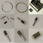
I only use Honeycomb Mobius construction for both, wire wound resistors and Mobius loops. The Mobius loops (same construction but using copper wire) help to clean up the signal in highly critical signal paths by manipulating the flow of electrical charge. The Honeycomb Mobius resistors already have this property.
The latest TDA1541A-MK6 prototype has multi-segment Honeycomb Mobius construction to further reduce self capacitance.
The resistors are made out of thin insulated resistance wire. I mainly use 63 Ohms / meter and 100 Ohms / meter. So a 500 Ohm I/V resistor would require 5 meters of 100 Ohm / meter resistance wire.
The resistor is made non-inductive by folding the wire half way in order to make a Mobius loop. This way the magnetic fields created around each wire are canceled, reducing inductance to almost zero. You could basically fold the wire, twist it using a hand drill and wind it on a former.
But wire wound resistors also have self capacitance. In order to minimize this self capacitance, winding methods can be used that either increase the distance between the wires, or minimize the surface area where the wires cross. Suitable winding method for this is the honeycomb winding pattern. The distance between parallel wires is increased to the wire diameter and the area where the wires cross is also minimized.
The latest experimental version is a multi-segment Honeycomb construction where the self capacitance of each segment is reduced by factor 3. Example, if each segment has 30pF stray capacitance, then the 3-segment assembly offers 10pF stray capacitance, this is caused by series connection of the stray capacitances. These resistors are difficult to construct, as the 3 separate windings must be made with one un-interrupted piece of resistance wire. markings are placed on 1/3 and 2/3 of the folded wire length to indicate when to move to the next segment. I attached a photograph of 3-segment Honeycomb Mobius resistors used in the latest TDA1541A-MK6 module.
In order to create a honeycomb pattern we need discs with an odd number of petals, I use 11 petals. I constructed the frame from 2 pieces of CNC milled PCB material and a 15mm plastic spacer.
I attached a second picture illustrating the winding process. I get the wire in 5 meter lengths, first I solder both wire ends and measure if the resistance is 500 Ohms or higher. This prevents frustration when the resistor is completed and the measured value turns out to be too low. For achieving maximum performance it is important to use one single un-interrupted wire.
Double spool holder ensures the wire doesn't get entangled during winding, so one can fully concentrate on the winding process. I made it from aluminum parts and two empty copper wire spools. The wires are guided using a white nylon plastic block with two small holes drilled in it.
One end of the wire is fixated to spool #1 using sellotape. The wire end is folded back over the tape so it won't slip through when wire tension increases. The wire is carefully wound on spool #1. Next the other end is fixated to spool #2 in a similar way.
The wire is then pulled off the spool and the end of the loop (2.5 meters) is fixated to a counterweight (I use rubber sheet). This counter weight keeps tension on the wires when winding the wire back on both spools. When ready we have same wire length on both spools.
Next the honeycomb frame is fixated using a M3 screw and a hexagonal brass spacer as illustrated.
The fold is placed on a lower petal (disc closest to the brass spacer). Then both wire ends are wound on the frame, skipping 3 petals every time.
When completed both wire ends are temporarily fixated to the frame by winding it around the petals. The frame is now self supporting so the screw and hexagonal spacer can now be removed.
Now the resistance value can be fine-tuned by cutting off pieces of wire. In this example every cm of wire corresponds to 1 Ohm resistance. Both wires must have same length, so when cutting 1cm off one wire, the same has to be done with the other. After soldering the wire ends, the resistance can be re-checked. This process is repeated until the resistor value is correct.
Hi EC, Can you point me to the details/materials/process used to wind you I/V resistors please. I've looked back through the thread but cant find it. Thanks, Ian
I only use Honeycomb Mobius construction for both, wire wound resistors and Mobius loops. The Mobius loops (same construction but using copper wire) help to clean up the signal in highly critical signal paths by manipulating the flow of electrical charge. The Honeycomb Mobius resistors already have this property.
The latest TDA1541A-MK6 prototype has multi-segment Honeycomb Mobius construction to further reduce self capacitance.
The resistors are made out of thin insulated resistance wire. I mainly use 63 Ohms / meter and 100 Ohms / meter. So a 500 Ohm I/V resistor would require 5 meters of 100 Ohm / meter resistance wire.
The resistor is made non-inductive by folding the wire half way in order to make a Mobius loop. This way the magnetic fields created around each wire are canceled, reducing inductance to almost zero. You could basically fold the wire, twist it using a hand drill and wind it on a former.
But wire wound resistors also have self capacitance. In order to minimize this self capacitance, winding methods can be used that either increase the distance between the wires, or minimize the surface area where the wires cross. Suitable winding method for this is the honeycomb winding pattern. The distance between parallel wires is increased to the wire diameter and the area where the wires cross is also minimized.
The latest experimental version is a multi-segment Honeycomb construction where the self capacitance of each segment is reduced by factor 3. Example, if each segment has 30pF stray capacitance, then the 3-segment assembly offers 10pF stray capacitance, this is caused by series connection of the stray capacitances. These resistors are difficult to construct, as the 3 separate windings must be made with one un-interrupted piece of resistance wire. markings are placed on 1/3 and 2/3 of the folded wire length to indicate when to move to the next segment. I attached a photograph of 3-segment Honeycomb Mobius resistors used in the latest TDA1541A-MK6 module.
In order to create a honeycomb pattern we need discs with an odd number of petals, I use 11 petals. I constructed the frame from 2 pieces of CNC milled PCB material and a 15mm plastic spacer.
I attached a second picture illustrating the winding process. I get the wire in 5 meter lengths, first I solder both wire ends and measure if the resistance is 500 Ohms or higher. This prevents frustration when the resistor is completed and the measured value turns out to be too low. For achieving maximum performance it is important to use one single un-interrupted wire.
Double spool holder ensures the wire doesn't get entangled during winding, so one can fully concentrate on the winding process. I made it from aluminum parts and two empty copper wire spools. The wires are guided using a white nylon plastic block with two small holes drilled in it.
One end of the wire is fixated to spool #1 using sellotape. The wire end is folded back over the tape so it won't slip through when wire tension increases. The wire is carefully wound on spool #1. Next the other end is fixated to spool #2 in a similar way.
The wire is then pulled off the spool and the end of the loop (2.5 meters) is fixated to a counterweight (I use rubber sheet). This counter weight keeps tension on the wires when winding the wire back on both spools. When ready we have same wire length on both spools.
Next the honeycomb frame is fixated using a M3 screw and a hexagonal brass spacer as illustrated.
The fold is placed on a lower petal (disc closest to the brass spacer). Then both wire ends are wound on the frame, skipping 3 petals every time.
When completed both wire ends are temporarily fixated to the frame by winding it around the petals. The frame is now self supporting so the screw and hexagonal spacer can now be removed.
Now the resistance value can be fine-tuned by cutting off pieces of wire. In this example every cm of wire corresponds to 1 Ohm resistance. Both wires must have same length, so when cutting 1cm off one wire, the same has to be done with the other. After soldering the wire ends, the resistance can be re-checked. This process is repeated until the resistor value is correct.
Attachments
Last edited:
Ok, 74AUC1G74 soldered! The missing tool was the soldering wick. Now it's even easy.... Thank you again EC for the link to the instructive video.
Hi Favel,
Well that's progress, consider the positive side of it, you can still see the parts without needing a microscope.
Here is a good demonstration video of how to solder SMD
http://www.youtube.com/watch?v=3NN7UGWYmBYy
Hi all,
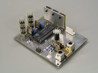
Yesterday i got my MK6 from John. I followed the route from MK1 to MK6. Heard every 'make'. I also did the Double Crown update with multi-segment I/V. The MK6 is, i do believe, really the final version. This is science from the highest grade. Bravo John!
How does the MK6 sound?: well, just 'right' in every part of the audio spectrum. That's all to say. If you want flavour, don't look at this dac. If you want to hear what's on a CD recording, nothing less and nothing more, you have to listen to this DAC and i am sure it will be your last for redbook audio. It's dead quiet and precise. All available bit information is present at the output without any phase distortion. Any noise level is absent. The resolution of the MK6 is stunning. Anyone who thinks that an modern OS DAC is needed to get all details have to hear this DAC. It's not the cheapest on the market, but you will get the highest feasible mix of non fatigue natural sound versus presentation of all real recording details.
The Double Crown with the multi-segment I/V gives a bit more definition against a non-s chip with single-segment I/V. I could live with both.
Hi all,
Yesterday i got my MK6 from John. I followed the route from MK1 to MK6. Heard every 'make'. I also did the Double Crown update with multi-segment I/V. The MK6 is, i do believe, really the final version. This is science from the highest grade. Bravo John!
brubeck -
I currently have the Mk.2 and I've been wondering about making the upgrade. Presumably the Mk.6 doesn't have such as low output impedance as Mk.2 since it has no output buffer? Also I'm a bit puzzled by the output of Mk.6 being referred to the 5V line rather than ground. Do you use yours with a conventionally grounded amp, and do you use John's recommended wirewound pot?
Regards, John.
A disadvantage which i experienced with the pre MK4 models was that they sounded thin. A preamp was needed to get full body sound. Since the use of a powerfet icm with the honeycomb I/V resistor this is solved. It's a huge difference! Do you use a powerfet output already? I think it is one of most important changes in the range. Taking signal ground from ground to 5V is easy to do and audible; it' s cleaner and more precise. The only thing to take care of is that the source is not connected to earth. Another new finding of John is to avoid the coupling cap and make a DC coupling. With the Powerfet output stage it is easily done with 2 diodes and a 2,5K potmeter. Between the dac and poweramp i only use a wirewound 1K potmeter for volume isn't that great a DC coupled DAC? It saves a lot of money for expensive coupling cap's and the result of dc-coupling is the best to get.
...... Do you use a powerfet output already? I think it is one of most important changes in the range. Taking signal ground from ground to 5V is easy to do and audible; it' s cleaner and more precise. The only thing to take care of is that the source is not connected to earth.
Thanks for replying.
No, I don't have the powerfet output - my version uses jfets and the jfet buffer.
Regarding the output, do I understand that you mean it's OK to connect the 5V line to amp earth because the 5V is floating?
I'll email John about a possible upgrade. I hope this is really the final final version!
")
Hi jonners,
The MK6 output impedance equals 500 Ohms. This is already lower than the output impedance offered by most audiophile tube pre amplifiers.
All buffers add distortion and much more important, limit resolution, that's why I had to remove them in the MK6.
The MK6 output signal (2Vpp) is directly generated across a 500 Ohm passive I/V resistor. The current buffer (lateral power MOSFET) forms a grounded gate buffer circuit. It presents a low impedance to the DAC output (approx. 12 Ohms) and a high impedance to the I/V resistor. It simply passes the DAC output current to the passive I/V resistor since the gate current is virtually zero. At the output of the buffer we have the same DAC current, but now without output compliance. This means we could generate say 100Vpp across a passive I/V resistor when using suitable I/V resistor supply and 25K Ohm I/V resistor.
The I/V resistor connects to +5V (it is best to feed all bit currents back to the +5V power supply). This minimizes ripple current on the +5V power supply.
The signal is present across the I/V resistor or +5V and output. That's why I used +5V as GND reference.
When using GND as reference, the output signal has to make a bigger loop that includes the +5V power supply and its imperfections:
output > load > GND > +5V.
When using +5V as reference the output signal makes a smaller loop:
output > load > +5V
The voltage drop across the I/V resistor equals 0.002 * 500 = 1V DC. So we would require a coupling cap. Recent tests showed the obvious, there is no perfect coupling cap, so the coupling cap adds distortion and limits resolution. Most isolation transformers can't handle DC so the coupling cap remains necessary.
In general, the coupling caps achieved better approximation to DC coupling compared to isolation (I/V) transformers.
By adding a 1V reference voltage that is connected to +5V the DC voltage between this reference voltage and DAC output equals zero. Then we can finally get rid of the coupling cap.
In practice a silicon diode (approx. 0.6V) and a Schottky diode (approx. 0.4V) connected in series give approx. 1V drop. With sufficient bias current the diodes present a very low impedance (short circuit) for ac signals. I try to avoid the use of electrolytic caps as these color the sound. Experiments with emitter followers and OP-amps failed as they caused poor sound quality compared to the diode solution. I suspect (local) feedback loops.
Presumably the Mk.6 doesn't have such as low output impedance as Mk.2 since it has no output buffer?
The MK6 output impedance equals 500 Ohms. This is already lower than the output impedance offered by most audiophile tube pre amplifiers.
All buffers add distortion and much more important, limit resolution, that's why I had to remove them in the MK6.
Also I'm a bit puzzled by the output of Mk.6 being referred to the 5V line rather than ground.
The MK6 output signal (2Vpp) is directly generated across a 500 Ohm passive I/V resistor. The current buffer (lateral power MOSFET) forms a grounded gate buffer circuit. It presents a low impedance to the DAC output (approx. 12 Ohms) and a high impedance to the I/V resistor. It simply passes the DAC output current to the passive I/V resistor since the gate current is virtually zero. At the output of the buffer we have the same DAC current, but now without output compliance. This means we could generate say 100Vpp across a passive I/V resistor when using suitable I/V resistor supply and 25K Ohm I/V resistor.
The I/V resistor connects to +5V (it is best to feed all bit currents back to the +5V power supply). This minimizes ripple current on the +5V power supply.
The signal is present across the I/V resistor or +5V and output. That's why I used +5V as GND reference.
When using GND as reference, the output signal has to make a bigger loop that includes the +5V power supply and its imperfections:
output > load > GND > +5V.
When using +5V as reference the output signal makes a smaller loop:
output > load > +5V
The voltage drop across the I/V resistor equals 0.002 * 500 = 1V DC. So we would require a coupling cap. Recent tests showed the obvious, there is no perfect coupling cap, so the coupling cap adds distortion and limits resolution. Most isolation transformers can't handle DC so the coupling cap remains necessary.
In general, the coupling caps achieved better approximation to DC coupling compared to isolation (I/V) transformers.
By adding a 1V reference voltage that is connected to +5V the DC voltage between this reference voltage and DAC output equals zero. Then we can finally get rid of the coupling cap.
In practice a silicon diode (approx. 0.6V) and a Schottky diode (approx. 0.4V) connected in series give approx. 1V drop. With sufficient bias current the diodes present a very low impedance (short circuit) for ac signals. I try to avoid the use of electrolytic caps as these color the sound. Experiments with emitter followers and OP-amps failed as they caused poor sound quality compared to the diode solution. I suspect (local) feedback loops.
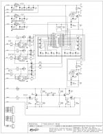
Hi fvale,
The problem is that multiple loads connected to one master clock output will interfere. So a noisy circuit that is connected to the same master clock output can pollute both, the master clock, and the critical circuits that connect to the same master clock output.
Clock buffers cannot fully prevent this (stray capacitance), and worse, add jitter (propagation delay).
So I now use a balanced (synchronized) master clock, based on 2 choke-loaded lateral power MOSFET source followers. These source followers also act as clock buffers (avoiding extra propagation delay of additional clock buffers).
Both source followers connect through multiple crystals in series (filter). This gives highly effective separation of both connected clock loads.
I added concept schematics of the TDA1541A-MK6 DAC, this is not exactly the same as the final version but it illustrates both master clock and clock distribution.
It also shows the lateral power MOSFET current buffers that fix the TDA1541A output compliance.
It's enough to simply connect in parallel the 11Mhz output going to decoder IC and 74AUC1G74 reclocker (schematic at post #3465)? Or is it better to "decouple" loads somehow? Thanks.
The problem is that multiple loads connected to one master clock output will interfere. So a noisy circuit that is connected to the same master clock output can pollute both, the master clock, and the critical circuits that connect to the same master clock output.
Clock buffers cannot fully prevent this (stray capacitance), and worse, add jitter (propagation delay).
So I now use a balanced (synchronized) master clock, based on 2 choke-loaded lateral power MOSFET source followers. These source followers also act as clock buffers (avoiding extra propagation delay of additional clock buffers).
Both source followers connect through multiple crystals in series (filter). This gives highly effective separation of both connected clock loads.
I added concept schematics of the TDA1541A-MK6 DAC, this is not exactly the same as the final version but it illustrates both master clock and clock distribution.
It also shows the lateral power MOSFET current buffers that fix the TDA1541A output compliance.
Attachments
Last edited:
- Home
- Source & Line
- Digital Line Level
- Building the ultimate NOS DAC using TDA1541A