Hi ernesternest,
I use 10K in parallel with 27K (7.3K).
Have you got a hint for R9 to get -15 V out of your 7915 replacement circuit.
I use 10K in parallel with 27K (7.3K).
Hi ernesternest,
I use 10K in parallel with 27K (7.3K).
THX! Looking forward to building it! And then to hearing it

Cheers Ernst
Hi fvale,
You could use 1N4148 for BAS16 and BAT43 for BAT17.
Do through hole alternative diodes exists for BAS16 and BAT17? I usually work with pre-drilled pcbs and my usual supplier has no stock for BAT17. Thank you.
You could use 1N4148 for BAS16 and BAT43 for BAT17.
Thank you Ecdesigns! I've another question about clock dividers. In my TDA1540 based cd player I used an about 8MHz clock generator followed by a 74HC74 to get the required 4MHz. Now I want to add another 74HC74, two stages used, in order to get 1MHz to directly feed BCK on the DAC. Is the 74HC74 a good choice for this purpose?
Hi fvale,
The 74HC74 dual flip-flop has high on-chip ground-bounce and is too slow (propagation delay) to achieve required low jitter levels.
I use these in the TDA1541A-MK5:
TEXAS INSTRUMENTS|SN74AUC1G74DCUR|LOGIC, 74AUC1G, D FLIP FLOP, US8 | Farnell Nederland
This causes cumulative jitter (jitter of each flip flop is added).
It would be better to apply synchronous reclocking of the derived BCK signal. Then there is mainly propagation delay induced jitter of one single flip flop plus masterclock intrinsic jitter.
With a 74AUC1G74 synchronous reclocker you would have masterclock intrinsic jitter plus 7ps (typical) ... 12ps (max.) peak to peak jitter.
With 3 cascaded 74HC74 flip flops you would have masterclock intrinsic jitter plus approx. 510 ps (typical) ... 1050 ps (max) peak to peak jitter.
Is the 74HC74 a good choice for this purpose?
The 74HC74 dual flip-flop has high on-chip ground-bounce and is too slow (propagation delay) to achieve required low jitter levels.
I use these in the TDA1541A-MK5:
TEXAS INSTRUMENTS|SN74AUC1G74DCUR|LOGIC, 74AUC1G, D FLIP FLOP, US8 | Farnell Nederland
Now I want to add another 74HC74, two stages used, in order to get 1MHz to directly feed BCK on the DAC.
This causes cumulative jitter (jitter of each flip flop is added).
It would be better to apply synchronous reclocking of the derived BCK signal. Then there is mainly propagation delay induced jitter of one single flip flop plus masterclock intrinsic jitter.
With a 74AUC1G74 synchronous reclocker you would have masterclock intrinsic jitter plus 7ps (typical) ... 12ps (max.) peak to peak jitter.
With 3 cascaded 74HC74 flip flops you would have masterclock intrinsic jitter plus approx. 510 ps (typical) ... 1050 ps (max) peak to peak jitter.
So, if I correctly understand, a 74AUC1G74 can be used as a 74HC74. I could use one to get my main 4MHz clock, followed by a second one and a third one cascaded to get 1MHz BCK. Then another one to synchronously reclock BCK (and other two for WS and DATA). Right? Many thanks again!
Hi fvale,
You will need 2 x 74AU1G74 to replace one 74HC74 as this chip contains 2 D flip-flops.
This is possible. If the I2S source signals are clean enough, it's also possible to only use synchronous reclocking for BCK, WS and DATA.
So, if I correctly understand, a 74AUC1G74 can be used as a 74HC74
You will need 2 x 74AU1G74 to replace one 74HC74 as this chip contains 2 D flip-flops.
I could use one to get my main 4MHz clock, followed by a second one and a third one cascaded to get 1MHz BCK. Then another one to synchronously reclock BCK (and other two for WS and DATA). Right? Many thanks again!
This is possible. If the I2S source signals are clean enough, it's also possible to only use synchronous reclocking for BCK, WS and DATA.


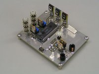
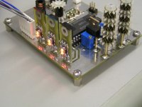
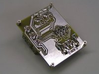
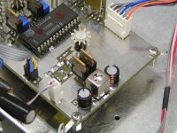
TDA1541A-MK6 prototype completed.
Hi galeb,
Here's another,
Yesterday I completed a TDA1541A-MK6 prototype PCB, see attached pictures.
The module is small, it only measures 94 x 72mm.
The discrete voltage regulator properties allowed removing all electrolytic capacitors and LC filters on the PCB.
The module basically contains +5V, -5V, and -15V discrete regulators, balanced masterclock, I2S synchronous reclockres, balanced DEM synchronizer, TDA1541A, and output stages.
The balanced masterclock is built around two power MOSFETs, two matched crystals, and two multi-segmented air chokes. The multi-segment construction lowers choke self capacitance. Masterclock output signals are rectified using RF Schottky diodes. Masterclock is powered from +5V using a RC filter. The resistor is a 40 Ohms Honeycomb Mobius resistor for maintaining low noise levels.
The synchronous reclocers are also powered through RC filters, 680 Ohms for the bit reclocker / DEM synchronizer and 1K5 for DATA and WS reclockers.
The 14 1206 size SMD film decoupling caps are mounted underneath the TDA1541A.
The output stage is the latest grounded gate MOSFET current buffer driving a 500R passive I/V resistor. MOSFET gate voltage can be adjusted with a trimmer in order to set required DC voltage at the DAC outputs. SMD 1uF film caps were used for gate decoupling. TDA1541A outputs are loaded with 220pF 805 size SMD film caps, this minimizes RF / HF noise and glitches.
The passive I/V resistors were further optimized (lower self capacitance) by using multi-segmented Mobius Honeycomb wire wound resistors. Plain twisted Mobius loop (non-inductive) of 5 meter wire results in approx. 270pF self capacitance. The Mobius Honeycomb construction reduces this to approx. 94pF. The multi-segmented construction consists of 3 segments with approx. 45pF each. This results in approx. 15pF self capacitance.
The I/V resistor low self capacitance allows for higher external capacitive loading (interlinks) and offers improved sound quality.
The coupling caps are placed externally. I am using 6.6uF charge compensated Mobius Hybrid caps at the moment. These offer improved performance at low level voltage changes and reduce typical film cap distortion.
In order to prevent ground loops when connecting external equipment like power amps, 1 : 1 or 1 : 1 : 1 studio isolation transformers can be used. These can also provide balanced outputs.
Hi galeb,
I see 1541 everywhere.......
Here's another,
Yesterday I completed a TDA1541A-MK6 prototype PCB, see attached pictures.
The module is small, it only measures 94 x 72mm.
The discrete voltage regulator properties allowed removing all electrolytic capacitors and LC filters on the PCB.
The module basically contains +5V, -5V, and -15V discrete regulators, balanced masterclock, I2S synchronous reclockres, balanced DEM synchronizer, TDA1541A, and output stages.
The balanced masterclock is built around two power MOSFETs, two matched crystals, and two multi-segmented air chokes. The multi-segment construction lowers choke self capacitance. Masterclock output signals are rectified using RF Schottky diodes. Masterclock is powered from +5V using a RC filter. The resistor is a 40 Ohms Honeycomb Mobius resistor for maintaining low noise levels.
The synchronous reclocers are also powered through RC filters, 680 Ohms for the bit reclocker / DEM synchronizer and 1K5 for DATA and WS reclockers.
The 14 1206 size SMD film decoupling caps are mounted underneath the TDA1541A.
The output stage is the latest grounded gate MOSFET current buffer driving a 500R passive I/V resistor. MOSFET gate voltage can be adjusted with a trimmer in order to set required DC voltage at the DAC outputs. SMD 1uF film caps were used for gate decoupling. TDA1541A outputs are loaded with 220pF 805 size SMD film caps, this minimizes RF / HF noise and glitches.
The passive I/V resistors were further optimized (lower self capacitance) by using multi-segmented Mobius Honeycomb wire wound resistors. Plain twisted Mobius loop (non-inductive) of 5 meter wire results in approx. 270pF self capacitance. The Mobius Honeycomb construction reduces this to approx. 94pF. The multi-segmented construction consists of 3 segments with approx. 45pF each. This results in approx. 15pF self capacitance.
The I/V resistor low self capacitance allows for higher external capacitive loading (interlinks) and offers improved sound quality.
The coupling caps are placed externally. I am using 6.6uF charge compensated Mobius Hybrid caps at the moment. These offer improved performance at low level voltage changes and reduce typical film cap distortion.
In order to prevent ground loops when connecting external equipment like power amps, 1 : 1 or 1 : 1 : 1 studio isolation transformers can be used. These can also provide balanced outputs.
Attachments
Last edited:
Hi ECD,
Why did you've left the 4 crystal design?, I've got the best results with this con figuration. With 4 crsytals physically placed in different ways, you can partially anulate the XYZ dimensions vibrations, and increment the Q factor, and of course, reduce the phase noise thanks to a better frequency stability. And if you use some kind of temperature comensation circuitry, you can reduce Allan variation too.
Respect to the MK6 PCB, I like it a lot, specially DR. You are going to the final of the way of optimizing this design. Eventually, you've realized that DR are far better than integrated ones, not in regulation but in noise.
Best regards,

Problem with Mosfet output stage
Hi Ecdesigns,
I just made your latest version of DAC output stage in reply #3539.
But it has no sound from my speakers.
I've use 2SK2232 instead of 2SK2391, other parts use same value as yours.
+5V and -10V normally appear.
Which part that I should check for bring it to life?
Thanks & regards,
Hi Ecdesigns,
I just made your latest version of DAC output stage in reply #3539.
But it has no sound from my speakers.
I've use 2SK2232 instead of 2SK2391, other parts use same value as yours.
+5V and -10V normally appear.
Which part that I should check for bring it to life?
Thanks & regards,
Hi MamyPoko,
1) Check MOSFET connections, when viewing printed text on the device, pins facing down, left pin goes to wiper of P1, center pin goes to E3, right pin goes to DAC output.
2) Make sure to trim P1 / P2 for 0 ... -50mV DC measured between TDA1541A output (pin 6 / 25) and GND.
Output coupling caps need to be used to block DC (not shown on schematics).
Hi Ecdesigns,
Thanks for your reply.
Now my DAC can sing again.
I've use probe measure the wrong point, so I can't adjust offset voltage to 0V between pin 6/25 and ground.
Sound from your latest DAC I/V stage surprising me, it's improve sound of my system too much.
Thanks again for your good stuff that share to everybody.
Hi MamyPoko,
P1 sets the bias current through the Circlotron output stage. It's easiest to use a cheap energy cost meter that has an indication for power consumption (watts). Make sure P1 is set to its maximum value before powering up.
and then slowly turn P1 until the meter indicates approx. 11 watts. Make sure to use a high quality multi turn pot for P1.
P2 sets the DC offset on the output, adjust for 0V DC. It may be necessary to repeat P1 adjustment after adjusting P2.
200 ... 500mW.
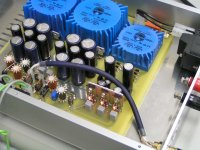
I attached a photograph of the latest version of the circlotron power amp.
- How to measure and adjust P1 and P2?
P1 sets the bias current through the Circlotron output stage. It's easiest to use a cheap energy cost meter that has an indication for power consumption (watts). Make sure P1 is set to its maximum value before powering up.
and then slowly turn P1 until the meter indicates approx. 11 watts. Make sure to use a high quality multi turn pot for P1.
P2 sets the DC offset on the output, adjust for 0V DC. It may be necessary to repeat P1 adjustment after adjusting P2.
- How much power rating of R16 and R17?
200 ... 500mW.
Could you please post your photo of your circlotron amplifier?
I attached a photograph of the latest version of the circlotron power amp.
Attachments
Hi galeb,
This was changed when switching to a balanced master clock. However, the balanced master clock can also run on 4 crystals.
I tested a balanced MOSFET 4-crystal master clock version some days ago in the latest TDA1541A-MK6 module. I soldered 4 matched cylindrical crystals together and connected them in series, keeping the wires as short as possible. The remaining 2 wires were soldered in the PCB. The crystal housings were connected with GND using a third wire. The crystals were screened using an IF transformer shield. I attached a picture.
The module sound quality was already very close to that of analogue sources. The typical "digital" sound already vanished after the many modifications I made to my audio set over the past months.
After switching from 2 to 4 crystals, there was the impression that a very slight "edge" that must still have been present in the sound, disappeared. Although not directly audible, it seems the sound is "stress free" now. This is based on extended listening tests that don't cause listening fatigue but even invite to keep on listening.
The properties of each oscillator change with temperature, this could lead to constantly varying pitch, jitter spectrum and noise spectrum. When multiple oscillators are used, it is very difficult to completely eliminate interference between these oscillators.
Practical example is an (SPDIF) source driving a Sabre DAC with local 80MHz crystal oscillator. Both clock signals enter a piece of silicon, then try to avoid inter-modulation between both clocks.
I experienced similar problems long time ago when experimenting with the microprocessor controlled tracker (basically a DPLL). I finally had to abandon this concept as I wasn't able to prevent inter-modulation between both source clock (SPDIF / I2S) and local VCXO. The result was that source jitter still managed to seep through.
This is why I decided to drive both, digital audio source and DAC with one and the same master clock, and use a I2S interface (no signal conversion). This way inter-modulation between both source and DAC clocks are avoided as there is little left to inter-modulate with. This concept also requires integration of both source and DAC using shortest possible clock and I2S interconnects.
But even when D/A conversion jitter would be zero, there is still the problem of clock jitter during A/D conversion and the fact that both studio and DAC clocks don't share the same time domain.
Why did you've left the 4 crystal design?, I've got the best results with this con figuration. With 4 crsytals physically placed in different ways, you can partially anulate the XYZ dimensions vibrations, and increment the Q factor, and of course, reduce the phase noise thanks to a better frequency stability. And if you use some kind of temperature comensation circuitry, you can reduce Allan variation too.
This was changed when switching to a balanced master clock. However, the balanced master clock can also run on 4 crystals.
I tested a balanced MOSFET 4-crystal master clock version some days ago in the latest TDA1541A-MK6 module. I soldered 4 matched cylindrical crystals together and connected them in series, keeping the wires as short as possible. The remaining 2 wires were soldered in the PCB. The crystal housings were connected with GND using a third wire. The crystals were screened using an IF transformer shield. I attached a picture.
The module sound quality was already very close to that of analogue sources. The typical "digital" sound already vanished after the many modifications I made to my audio set over the past months.
After switching from 2 to 4 crystals, there was the impression that a very slight "edge" that must still have been present in the sound, disappeared. Although not directly audible, it seems the sound is "stress free" now. This is based on extended listening tests that don't cause listening fatigue but even invite to keep on listening.
The properties of each oscillator change with temperature, this could lead to constantly varying pitch, jitter spectrum and noise spectrum. When multiple oscillators are used, it is very difficult to completely eliminate interference between these oscillators.
Practical example is an (SPDIF) source driving a Sabre DAC with local 80MHz crystal oscillator. Both clock signals enter a piece of silicon, then try to avoid inter-modulation between both clocks.
I experienced similar problems long time ago when experimenting with the microprocessor controlled tracker (basically a DPLL). I finally had to abandon this concept as I wasn't able to prevent inter-modulation between both source clock (SPDIF / I2S) and local VCXO. The result was that source jitter still managed to seep through.
This is why I decided to drive both, digital audio source and DAC with one and the same master clock, and use a I2S interface (no signal conversion). This way inter-modulation between both source and DAC clocks are avoided as there is little left to inter-modulate with. This concept also requires integration of both source and DAC using shortest possible clock and I2S interconnects.
But even when D/A conversion jitter would be zero, there is still the problem of clock jitter during A/D conversion and the fact that both studio and DAC clocks don't share the same time domain.
Attachments
- Home
- Source & Line
- Digital Line Level
- Building the ultimate NOS DAC using TDA1541A