What Charge Pump? [kidding]
I did it! I have -3.4V on the ES9023 NEG pin, no charge-pump cap. I do not have anything but a VOM handy so I hesitate to tweak the -V any more than I have. The SOUND? As good or better than before I started, and that is with no filtering on the POT wiper {yet}
9V battery [8.something] --> 79L05 --> 100R multi-turn POT, wiper set under load to -3.4Vdc [my prior NEG with +3.6 source and 100K to GND on ES9026 pin #6]
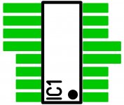
From this experience I would say it is worth determining what is the best negative voltage to place there. Now, mind you, my UAE23 device under test has 100K ohms on the Vreg pin ES9023 pin #6 to ground -- I could remove THAT however that is something I pretty much like, not having tried ESS suggestion of 130K or ODAC value of 118K there [100K is what I had when I did it].
SO that is another test yet to consider, a temporary POT {wired as variable R} and fixed-R on ES9023 pin #6 to ground so could have say 75K--200K test range. Test with a very "hot" recording like a female vocalist up close on the microphone example Musica Nuda.
I am currently playing The Bridge by Jens KrÜger and it sounds superb. The FET tester is not getting it's 9V back anytime soon")
What about the charge pump cap? I like the new XO placement a lot. I also like the now missing optional C103/C104 as you can tell from my beta build.
I did it! I have -3.4V on the ES9023 NEG pin, no charge-pump cap. I do not have anything but a VOM handy so I hesitate to tweak the -V any more than I have. The SOUND? As good or better than before I started, and that is with no filtering on the POT wiper {yet}
9V battery [8.something] --> 79L05 --> 100R multi-turn POT, wiper set under load to -3.4Vdc [my prior NEG with +3.6 source and 100K to GND on ES9026 pin #6]
From this experience I would say it is worth determining what is the best negative voltage to place there. Now, mind you, my UAE23 device under test has 100K ohms on the Vreg pin ES9023 pin #6 to ground -- I could remove THAT however that is something I pretty much like, not having tried ESS suggestion of 130K or ODAC value of 118K there [100K is what I had when I did it].
SO that is another test yet to consider, a temporary POT {wired as variable R} and fixed-R on ES9023 pin #6 to ground so could have say 75K--200K test range. Test with a very "hot" recording like a female vocalist up close on the microphone example Musica Nuda.
I am currently playing The Bridge by Jens KrÜger and it sounds superb. The FET tester is not getting it's 9V back anytime soon
What about the charge pump cap? I like the new XO placement a lot. I also like the now missing optional C103/C104 as you can tell from my beta build.
Since it turned out
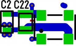
eek that a suitable pad layout for the ES9023 was not available I made a new one. Some pads are a little bit longer in order to put Cs directly at the pins For the charge pump 1-2.2µF X7R (0402 or 0603) is perfectly suited.Have a look at the layout for the XO decoupling and grounding. The small cap C22 for local decoupling (10nF COG/NPO) is as close a possible to VDD. GND is routed with a low impedance trace to the Cap. Note that only the bigger cap C2 (e.g. 2.2µF) is connected to the groundplane. The XO will draw current during rising or trailing edge. This will be delivered only from C22 (C2 is too slow and too far away) and thus the current will flow from C22 through the XO and back to C22. All the noise will stay there and not affect the main ground! I used the same layout for the flipflops
I omitted the TH foil caps (103, 104) since I am convinced that the SMD PPS caps are really good here and this gave some more room for improvements on the lower board area
BTW: I will clean the part numbering for the final version (e.g. order part numbers according to placement within schematic). Still a lot of work...
Have fun!
Attachments
As to the charge-pump and noise, as I told Daniel in another thread, I'll try and look for the prior noise he saw on the NEG pin around 1.5MHz...{amplitude unknown} Daniel expects there could be CP-related noise yet, with CP cap missing and NEG fed with -3.4Vdc. Only one way to tell, I have to look. I tried to Google charge-pump circuits and found "too many". I can only guess what is inside ES9023. I had another odd thought, not knowing the circuit inside....could I use a cap to ground on one or both of the CP pins I depopulated for the external NEG test? SWAMP it? 100R to GND? It's only a test and a crude one. I have a stack of SMD caps on the NEG pin to ground, ok, some mm away, I COULD make a very short path NEG --||--GND top-side on the UAE23 [another model of ES9023-based DAC sold on eBAy]. Maybe 0.01uF? .1? I can haul a scope up to the living room but maybe not on a Saturday evening, I've come too far not to get an answer as to the nature of the NEG pin and noise.
Good reasons to drop C103, C104. I had noticed the close proximity of C2, C22. That sounds like a good way to go, possibly even overkill, but that would not hurt. The longer pads around the ES9023 are a neat idea. I can't wait to try that version.
One additional question: how about moving the u.fl for MCLK closer to the ES9023 into the left part of the open space above the three other u.fl connectors? They don't really need to be in one line and that way the distance to the XO / ES9023 would be even shorter.
One additional question: how about moving the u.fl for MCLK closer to the ES9023 into the left part of the open space above the three other u.fl connectors? They don't really need to be in one line and that way the distance to the XO / ES9023 would be even shorter.
Ferrite bead in series to V+ to OSC? Should I2s lines have same length if MCK is used? {USB receiver}. I LOVE the new custom ES9023 pads!! Would ES9023 benefit in any way from a ground plate on top of it as shown in ES9018 thread? A swatch of copper foil and some GND pads to tack it to topside?
Good reasons to drop C103, C104. I had noticed the close proximity of C2, C22. That sounds like a good way to go, possibly even overkill, but that would not hurt. The longer pads around the ES9023 are a neat idea. I can't wait to try that version.
One additional question: how about moving the u.fl for MCLK closer to the ES9023 into the left part of the open space above the three other u.fl connectors? They don't really need to be in one line and that way the distance to the XO / ES9023 would be even shorter.
Don't think that C2 + C22 are overkill. You'll need a fast cap (e.g. <100nF) to serve the current need of the XO (3ns rise time -> 333MHz + harmonics up to GHz!) and with this small cap the reg will not be stable (at least MIC needs some ESR as you also mentioned -> Tantal). Also reg is much too slow to reload the small cap between the transitions.
Moving the u.fl is an option that i will check. Please note that I designed the traces for the I2S lines to have 50Ohm impedance (trace thickness, gap between trace and GND, board thickness,...) so the lenght of the trace will only add some (minor) damping. BTW: if you don't need the external MCLK you should cut the trace close to the ES9023 to avoid reflections
Ferrite beads together with close Cs are used to clean power just before the reg and to prevent dirt e.g. coming from the XO to spread to other parts (the reg is "open" for HF). Frequencies on I2S lines are still quite low (<< GHz) so the same length should not be necessary here. Impedance is more important. GND isn't routed yet and will be also on top layer under ES9023. Though directly on board and not using a copper foilFerrite bead in series to V+ to OSC? Should I2s lines have same length if MCK is used? {USB receiver}. I LOVE the new custom ES9023 pads!! Would ES9023 benefit in any way from a ground plate on top of it as shown in ES9018 thread? A swatch of copper foil and some GND pads to tack it to topside?
Thats a point I am just thinking over anyway: the routing of VDD to mute pin. This might be reworked...
Last edited:
It's always difficult to communicate glitch free on a forum like this. I didn't mean to suggest overkill. I really like the C2 , C22 arrangement as proposed. As far as I can tell it could handle frequencies many times higher than the ones we're dealing with here. That's where the idea came in.
Is there a ferrite for the clock yet? After MCK clock regulator?
I have not gotten back to my NEG-pin noise measurement task, nor checked for what happens if I turn that POT [DC offset?]. How much of a SIN would it be to take -15 and borrow some minus V from it for NEG? [shhh, just wondering aloud]. I hope to see what V is IDEAL for NEG and that shows no offset anywhere given a +3.6V into the V+ side of the DAC [and NOT employing the charge-pump cap]. [VREG pin may have some impact] If 1.5Mhz noise present, could I swamp it to ground? Cap or R? [CP pins? to GND ] I plan to answer all this. For my use, I would have no problem injecting a -V if it helps. If the art makes it easy...I will not turn it down - It sounds really nice injecting NEG but maybe it did anyway. *<:^) Do we know how much current the normal ES9023 @ 3.6V draws on peaks with CP in place as normal? {or what the minus side would need?}
What are current PCB dimensions [Beta 2] in CM?
Thanks for your further testing!
There is a ferrite in front of the MCLK reg. After the reg it only makes sense if you supply several ICs (e.g. in front of each FF).
Not sure if it's a good idea to take -V from analog part supply. This could inject noise into the analog part and GND routing would be significantly compromized (In the new layout I am using a segmented GND plane):
PCB dimensions are the same.
I thought Ferrite to prevent any RF from sneaking back at regulator via clock's V+ messing with regulator?. Sort of a 2/3rds Pi filter. I'm fine whatever happens.
Borrowing -V just me being lazy, of course I can make a supply... the Xformers I have at 36Vct .8A $6 {WoW}!! I can hit another WallWart with a hammer and have xformer for -5 or -3.6 or -3.3... or -ADJ... or feed the whole low voltage side with a rail-splitter. Too soon to tell. If I can find the noise you originally spotted, and if I reduce it... well, I MAY have to put CP cap back, look for the 1.5Mhz noise, take cap off, inject -3.4 scope again... if noise yet but less, swamp the vacant CP pins [USA term for divert/bleed] via ~.1uF Ea to ground or R(s) to GND...brute force. I assume if I turn -V on NEG up and down I should see DC at DAC outs? If I do, I would null that with POT and take reading...but I have 100K on Vreg too...so to help the rest of us I may need to try no 100K, or try what YOU plan to use there...ESS = 130K ODAC 118K HiFiMEDIY no R... I like having some headroom, *if* I understand things correctly. I seem to like the Vreg R in place.
My HOPE is that if I find an offset situation, a standard increment -V regulator will work and not have DC offset situation. I do not mind -5 and a POT and cap but some people would.
Update: progress of next version
Hello all,
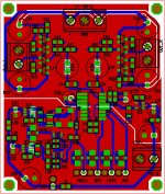
just want to give a short update of the actual progress of the next board version. Please find attached the actual layout. Note that the top layer ground plane (incl. all the vias) is not routed yet.
For the 3.6V reg I went for the MIC5205 with respect to bypass C layout (one C from BYP pin to ground). For the two 3.3V regs there is a second bypass C from BYP pin to OUT pin thus also other regs can be used (e.g. LT1761, heard that someone has lots of).
The XO was turned 90 degrees. The clock trace to ES9023 is a few mm longer (though impedance controlled 50Ohm) but I forgot the return current from ES9023 DGND pin to GND connection of C36. This way back was interupted before the 90 degrees turn by the ENABLE pin connection to SUPPLY pin of the XO which was routed on the bottom layer (damn HF)
I also introduced a segmented ground plane to keep the analog ground clean from digital noise. The connection is below the ES9023.
I will prepare a new BOM soon. This will also introduce the new component numbering.
Any comments, critics, recommendations,... are very welcome!
Hello all,
just want to give a short update of the actual progress of the next board version. Please find attached the actual layout. Note that the top layer ground plane (incl. all the vias) is not routed yet.
For the 3.6V reg I went for the MIC5205 with respect to bypass C layout (one C from BYP pin to ground). For the two 3.3V regs there is a second bypass C from BYP pin to OUT pin thus also other regs can be used (e.g. LT1761, heard that someone has lots of
).The XO was turned 90 degrees. The clock trace to ES9023 is a few mm longer (though impedance controlled 50Ohm) but I forgot the return current from ES9023 DGND pin to GND connection of C36. This way back was interupted before the 90 degrees turn by the ENABLE pin connection to SUPPLY pin of the XO which was routed on the bottom layer (damn HF)
I also introduced a segmented ground plane to keep the analog ground clean from digital noise. The connection is below the ES9023.
I will prepare a new BOM soon. This will also introduce the new component numbering.
Any comments, critics, recommendations,... are very welcome!
Attachments
Last edited:
About 825x LT1761 3.3v "around" yes. I have most of the parts for something like a group-buy of around 250x, but the FET matching I am not sure I would want to do. If you trust them, paying say a young kid to take the readings, might be an option.
Can you extend out a NEG pin pad to insert -V there? Else I would use top-mounted SMD C and fly in -V to it topside. I suspect I will make my OWN negative rail V as I did in the recent test: 79L05 or better, a POT, a cap. Micrel -3.6 might also work [the negative version of the +5209 model]. I am not done testing if there is DC offset on outs when I am flying in -3.4V to NEG pin [no CP cap{s}]. If there is DC OFFSET I could tune it out with my 10-turn PCB POT.
The segmented ground is nice, it would be even nicer if one could be ABLE to saw off the JG filter-buffer stage in a pinch, but eventually I WILL make the super tiny I2s ES9023 I am longing for. :^)
So there is regulator ART for FlipFlips{3.3V}, 50 clock{dedicated 3.3V}, and ES9023 {3.6}? Is there room for a ferrite between V+ to OSC and the LT1761? {am I nuts?}
I will probably use a 36Vct transformer and some lesser CT trans, so an outboard supply will have +/-15 and +/-5, the -5 I would derive NEG pin -V from [POT and CAP], if no fixed negative regulator is close enough.
A ground-isolated I2S isolator option at input could be slick ala Christian's Bragi board? IL715 [watch EXACTLY which model if you do; they come in various widths].
The last PCB vendor we used charges the same fee up to 10x10cm as 6x7
http://www.nve.com/Downloads/il71x.pdf
Isolators | Digital Isolators | DigiKey
I have a few Bragi boards, I could eventually try one with and one without the isolator.
Lovely, I don't see anything that I would want to change! The only exception to that is one label: I believe "GND" at the +15/-15 header is actually written "8ND", but then, maybe for a reason?
Glad that you like it
You have good eyes: it indeed looks like "8ND". Must be JPEG compression artefact since in my layout programm it reads "GND"Thank you very much for the feedback!
About 825x LT1761 3.3v "around" yes. I have most of the parts for something like a group-buy of around 250x, but the FET matching I am not sure I would want to do. If you trust them, paying say a young kid to take the readings, might be an option.
Can you extend out a NEG pin pad to insert -V there? Else I would use top-mounted SMD C and fly in -V to it topside. I suspect I will make my OWN negative rail V as I did in the recent test: 79L05 or better, a POT, a cap. Micrel -3.6 might also work [the negative version of the +5209 model]. I am not done testing if there is DC offset on outs when I am flying in -3.4V to NEG pin [no CP cap{s}]. If there is DC OFFSET I could tune it out with my 10-turn PCB POT.
What about using the C201 pins to connect to the NEG pin? If you have your dedicated -V supply you'll probably have a suitable cap "onboard"
The segmented ground is nice, it would be even nicer if one could be ABLE to saw off the JG filter-buffer stage in a pinch, but eventually I WILL make the super tiny I2s ES9023 I am longing for. :^)
Mmh, to be honest I don't see any reason to cut of the JG filter buffer as thats one of the main features of the boards
If you want to have it super tiny have a look at EUVLs excellent boards!So there is regulator ART for FlipFlips{3.3V}, 50 clock{dedicated 3.3V}, and ES9023 {3.6}? Is there room for a ferrite between V+ to OSC and the LT1761? {am I nuts}
ART? Yes, there are three dedicated regulators on board. One for the ES9023 (pin layout suitable for MIC5205 3.6V), one for the clock and one for the FFs. The latter two have two different alternative bypass C so that you can use both MIC5205 3.3 and LT1761 3.3 (or other compatible regs). There is a ferrite in front of the OSC reg to provide clean power to the reg and to prevent OSC noise spreading to other parts. Another ferrite between the reg and the OSC does not bring any further benefit. Thats different for the FFs, where one reg is supplying two FF. Here the ferrites decouple the two FF. Yes, you are nuts! (just a joke
) I will probably use a 36Vct transformer and some lesser CT trans, so an outboard supply will have +/-15 and +/-5, the -5 I would derive NEG pin -V from [POT and CAP], if no fixed negative regulator is close enough.
A ground-isolated I2S isolator option at input could be slick ala Christian's Bragi board? IL715 [watch EXACTLY which model if you do; they come in various widths].
The last PCB vendor we used charges the same fee up to 10x10cm as 6x7
http://www.nve.com/Downloads/il71x.pdf
Isolators | Digital Isolators | DigiKey
I have a few Bragi boards, I could eventually try one with and one without the isolator.
I want to keep the board simple and so I will probably not add isolators. To be honest I am not sure if those isolators are a real benefit. According to the datasheet they have 100ps pulse Jitter and max 3ns channel to channel skew. Thats in the range of the SDI/LRCLK set-up time to BCLK rising edge (t_DS = 2ns for the ES9023 as per the datasheet) so in the extreme situation you might have invalid SDI/LRCLK!. Not sure if this would be a real problem here but on the one hand we are discussing about clocks with jitter below 1ps and on the other hand...
USB isolators might be a different thing!One other quite trivial reason is I am using a freeware version of Target! with a maximum of component 250 pins and I am already using 240
- Status
- This old topic is closed. If you want to reopen this topic, contact a moderator using the "Report Post" button.
- Home
- Source & Line
- Digital Line Level
- Build thread for ES9023 + JG Buffer boards (betatest)