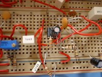

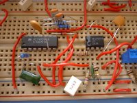
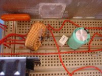
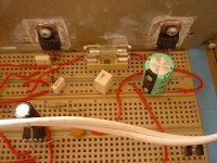
And again.....
I look forward to your comments. In particular i want to know if there is anything that can be done to improve survival of this circuit, the only weak point i am currently aware of is my tempory use of 1N1418 diodes to clamp the back emf from the inductor...
PS please excuse my spelling all
I look forward to your comments. In particular i want to know if there is anything that can be done to improve survival of this circuit, the only weak point i am currently aware of is my tempory use of 1N1418 diodes to clamp the back emf from the inductor...
PS please excuse my spelling all
Attachments
tade said:i like that your amp will have that built in distortion pedal!
In order to poke fun at his efforts, your own must be far more substantial, so I look forward to seeing it whenever you do get around to posting it.
Nitrate, I haven't gone over your schematics very closely but if you're clamping like I think you are those aren't the right kinds of diodes at all and you can just as easily take them out.
Don't expect people to be listing improvements for you, that will have to come with your own research and experimentation. One improvement to aim for is to go with dual N channels. How? Why? I can't tell you.
Fixing the filter, both cut off and component wise, would be my first step.
I'll soon be posting pics of my homebrew amp in the thread from which it originated, keep an eye out for it, I think you'll find it interesting.
Nicely done thus far, keep at it!
Chris
Feedback after the filter
Nitrate, thanks for posting the schematic.
I'm surprised that you take feedback from a point AFTER the filter. I've read that the phase shift introduced by the filter can cause oscillations and possibly instability. Most schematics I've seen put a voltage divider on the output from the MOSFETs and feed that back into the error amplifer.
How did you come up with your design? I've been meaning to build a full-bridge Class D with feedback, but I'm not very confident in my control theory.....
LOL
I knew i'd get comments about those 4148 diodes, i had a party last night, me and a few mates came back to my place after pub closing hours and we played music till 4am the next day. The amp was flat out all that time but the 4148's survived! bless them
Anyway just to put your minds at rest i'm gonna replace them now with some ultrafast high current diodes, namely MUR460RL. I have a a pack of these laying around and they should be ideal.
Some have noticed my feedback coming after the filter, this i have chosen to do to help eliminate the dodgeyness of the filter, it also helps to keep emf pulses out of the error amp stage. Belive me or not on this design the sound is much better this way, if i try taking the feedback from the bridge the high notes sound 'scratchy' and the scope shows high frequency interferenc on the output waveform. Maybe if i sort my inductor there will be less energy kicking around to cause this interference. Either way i like the idea of total global feedback, not just a shortcut from the bridge.
P channel fets are rare to say the least and changing my design to an all N channel is a wise move. I don't like the idea of bootstraping to create yet anougher power supply to drive the top fet, but i know its the right way to go, should mean i can use almost any high speed fet in the design.... i've already got hold of suitable driver chips from National Semis. Feels like i'm relying too on chip solutions though if i go down that route... Hmmm Besides i like maxim products because of their gaurantee of non obsolesence!
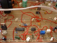
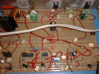
Somebody asked how i came up with the design, well i got reading this forum one day at work and i decided that i wanted to try class D for myself. I looked up on the net a description of class D amps so i knew what made them tick, then just sat down with a lump of breadboard and a scope and literally built one. I'm an electronic design engineer you see so thats what i do for a living, just sit down and build prototypes for to answer customers problems. Anyway i started by building a 275KHz clock. Origanally i used a 4093 i.c but the cmos familly aint fast enough. It ticked o.k but the square was not very square on the scope so i was forced to use high speed TTL family ( 74*** ) This also required the addition of a 5v supply. After the clock i added the next stage, the triangle. Easily done by way of anougher gate to buffer the clock then charge/discharge a cap from the output of the gate. I went to great lengths tweaking the values of the cap/resistor in order to obtain the purest triangle i could. When i was satified with the wave i then added the comparater, and a variable voltage divider. If all is well i should be getting a 50% pwm wave out the comparater. This checked out o.k so i decided to try sticking that into a p/n fet bridge across a 5v supply. This worked well so i tried stuffing a simple filter on the output ( actually the one i still use ) and hook up a speaker just to see what it sounded like. It was supprisingly good. I was using tiny e-line package fets to test it. After a succesfull test run i went to a bigger supply ( 12v ) and created a level shift circuit on the high side. This worked but the fets were getting quite hot even at idle. I found the drive was starting to get sloppy, Square was no longer square from the comparater so i tried squareing it up by buffering with anougher logic gate. This worked a bit but it eventually blew the logic. This is when i decided to use the maxim driver. Things were back up and running, but the fets were still a little warm. I just thought this was down to the small fets. Continued on next post....
I knew i'd get comments about those 4148 diodes, i had a party last night, me and a few mates came back to my place after pub closing hours and we played music till 4am the next day. The amp was flat out all that time but the 4148's survived! bless them
Anyway just to put your minds at rest i'm gonna replace them now with some ultrafast high current diodes, namely MUR460RL. I have a a pack of these laying around and they should be ideal.
Some have noticed my feedback coming after the filter, this i have chosen to do to help eliminate the dodgeyness of the filter, it also helps to keep emf pulses out of the error amp stage. Belive me or not on this design the sound is much better this way, if i try taking the feedback from the bridge the high notes sound 'scratchy' and the scope shows high frequency interferenc on the output waveform. Maybe if i sort my inductor there will be less energy kicking around to cause this interference. Either way i like the idea of total global feedback, not just a shortcut from the bridge.
P channel fets are rare to say the least and changing my design to an all N channel is a wise move. I don't like the idea of bootstraping to create yet anougher power supply to drive the top fet, but i know its the right way to go, should mean i can use almost any high speed fet in the design.... i've already got hold of suitable driver chips from National Semis. Feels like i'm relying too on chip solutions though if i go down that route... Hmmm Besides i like maxim products because of their gaurantee of non obsolesence!
Somebody asked how i came up with the design, well i got reading this forum one day at work and i decided that i wanted to try class D for myself. I looked up on the net a description of class D amps so i knew what made them tick, then just sat down with a lump of breadboard and a scope and literally built one. I'm an electronic design engineer you see so thats what i do for a living, just sit down and build prototypes for to answer customers problems. Anyway i started by building a 275KHz clock. Origanally i used a 4093 i.c but the cmos familly aint fast enough. It ticked o.k but the square was not very square on the scope so i was forced to use high speed TTL family ( 74*** ) This also required the addition of a 5v supply. After the clock i added the next stage, the triangle. Easily done by way of anougher gate to buffer the clock then charge/discharge a cap from the output of the gate. I went to great lengths tweaking the values of the cap/resistor in order to obtain the purest triangle i could. When i was satified with the wave i then added the comparater, and a variable voltage divider. If all is well i should be getting a 50% pwm wave out the comparater. This checked out o.k so i decided to try sticking that into a p/n fet bridge across a 5v supply. This worked well so i tried stuffing a simple filter on the output ( actually the one i still use ) and hook up a speaker just to see what it sounded like. It was supprisingly good. I was using tiny e-line package fets to test it. After a succesfull test run i went to a bigger supply ( 12v ) and created a level shift circuit on the high side. This worked but the fets were getting quite hot even at idle. I found the drive was starting to get sloppy, Square was no longer square from the comparater so i tried squareing it up by buffering with anougher logic gate. This worked a bit but it eventually blew the logic. This is when i decided to use the maxim driver. Things were back up and running, but the fets were still a little warm. I just thought this was down to the small fets. Continued on next post....
Amp birth continued......
I decided it was time to get serious so i got hold of the two big fets i use now, The IRF***'s. I put these in and powed up, all seemed well exept the fets where getting very hot very fast and the clarity of music had dropped. Shortly after this the maxim i.c died. I replaced the ic, and put resistors in line with the fet gates. This was to stop exessive current being draw through the driver i.c. I forgot to take into account fet transconductance. This stopped the driver blowing but the fets still ran very hot. I went searching for answers on the irf website when a came accross an application note that babbled on about class d amp design. I printed a copy off and read through it befor i went to bed. It was from that app note that i learnt about dead time and its affects on switching amp design. I realised then that it was this causing things to get hot and causing massive emf pulses and ringing in the switching stage. I presumed the fets were switching instantly and had totally neglected to take into account the fact that both devices were on at switch points. The next day i came home from work and lobbed a dead time delay circuit in the amp, making use of more of the 7414's gates. upon power up everything was fine again, sound quality was back and nothing was getting hot. Next i gingerly tried using split supply by adding an SLA battery the wrong way round on to the lower fets power rails. This gave +-12v across the bridge. I switched on and everything blew up! Hmm i thought. I looked around the board, there appeared to be a short somwere. I finally located a blown 4148 causing a short. I had forgotten to move its cathode on to the lower supply rail when i added it, it was still configured for single supply. I sorted this out, powed on and all was fine. After this i spent a few days playing with dead time and speeding up squares ect. Getting it nice and safe for the big supply test. When i was convinced nothing wold blow up i tried it on a real +-35V supply as i am using now. I crossed my fingers, quickly turned on then off the plug socket. Nothing fried, no burning smell, i felt around the board for hot components. Nothing. So i turned it back on at arms length and kept my finger hovering over the socket switch, poised ready to flick off the power. All seemed well. after a few seconds i reached for my meter and started checking all supplies n stuff. I let out a sigh of relefe. it was a success. I power down again, fitted a heatsink to the fets as they were warming up a little in free air, powered back up and injected some music. It was nice if not a little hissy with a background 100Hz hum
I modded the supply by adding a smothing resister and secondy cap resevoir, this sorted the mains hum. Then i turned my attention to getting rid of the hiss. After grounding the heatsink a lot of the hiss went away, but there was still a lot there so i added an error amp to the input stage. This completly silenced the amp whilst still giving me the full 75 watts on a signal of 2vPK-PK in. That is pretty much it, i hope that answers your question on how did i come up with the design. I suppose the design mostly designed itself out of nesecity. I'll leave out the bits about trying dual n-fets and blowing the whole back end out of the bread board n other little mishaps along the way
Hope you all enjoyed, i got a bit carried away there.
P.S Hope you americans stay safe in the storms
Mad.P
P.S Hope you americans stay safe in the storms
Thanks. I am glad your results have been good so far. I like how you used the Schmitt trigger inverter. It is my favorite.
A little guidance - glad to see people trying this on their own
"1. The whole of the amp runs COLD even after a good hammering, EXCEPT for one part, the output filter inductor, it always runs hot - WHY? "
If an inductor is warm, that means it is saturating. Your switching frequency is likely too low, or the voltage which you are integrsting is higher than originally intended for the inductor. Or, the switching frequency is too high for the core material. Try using Coilcraft DO3340 devices, they are very linear and are suitable for mid power amplifiers.
"3. I am using spec-matched complimentry fets for the output stage (( N & P type ) IRF9530, IRF520 ) When i run the amp at idle with no heat sink on the fets, the high side ( P ) fet gets slightly warmer than the low side, WHY? "
Physics, dude. The IRF matched devices have P channels with almost twice the on resistance. They are matching the analog performance, not the conductivity. Class D uses the FETs as switches. Keep your P Channel for medium power amplifiers, but plan on moving to N channels as you go above about 100W for best efficiency.
Just a note about the fets...
When i say i'm using a matched pair i didn't get them as a matched pair from the manufacturer, i pick two different types that had almost identicle specs, on resistance and max voltage, gate capacitance ect. The complementry part for the IRF520 is IRF9520, but the data sheet tells me they are an uneven match so i use IRF9530 instead. This according to its data sheet is almost identical. That is why i asked why the P channel runs warmer than the N channel. They have the same RDS when fully on so i think there must be more going on than the obvious
Its not a problem, i just preferr to know whats going on so i can be safe when building at higher powers.
Mad.P
Congrats on a working circuit.
There are three things I would personally change:
Use a Miller integrator to make your rectangular -> triangular conversion (this would give a more linear ramp than from a 1st order LPF).
Make a parallel DC path to your AC coupled gate-drive so you can drive your amp into clipping without getting latched up (BTW the diodes are OK that way in my experience).
You are lucky that your amp is stable with post-filter NFB without taking any particular precautions. The total transfer function of the loop should be like a first order lowpass and the whole loop should be DC coupled.
Regards
Charles
Hi,
Without the intention of offending anyone or their hard work in any way at all, I think a few of these homebrew amps we've been seeing very recently, such as this, is exactly what I meant when I said even a bad class d sounds impressively good.
This leads me into a new thread, hope to see you there!
Chris
Ouroboros said:The output filter core has a very hard life in a class-D amp. I've tried dust-iron toroidal cores (such as you might use in a buck regulator) and they get very hot. Good quality open-bobbin ferrite inductors work well, but they have a large external field that can cause a lot of problems with magnetic induction on the pcb. There are a few companies now selling precision-gapped ferrite toroids for class-D applications. They are expensive and I've not had the chance to try one yet, but they should work well.
What about ferrite cans? ferrite are said to be much cooler at high frequency, and can type cores have low emission.
ps: cores get heated at high frequency, it has nothing to do with satuation.
I have recently tested a 10 watt BJT transistor class D (THD around 1%) and now I'm planning to build something like yours (75 watt IRF 530/9530 half bridge, but UcD-like self oscillation).
IMHO, the next thing to do (for you ) is:
Remove the clamping 4148 (probably they wouldn't turn on at all)
Replace the LM358 and 393 with some faster device like NE5532 plus LM311. (358 is too slow even for linear amplifiers)
Build a PCB or at least solder a "hole board"
Fix the filter
Use some calculated feedback control scheme (your post-LPF NFB seems not reliable, it may cause oscillation around resonance frequency of the LC circuit -- high voltage dangerous! )
 Add some firm diode clamping at the output to prevent the HV danger -- perhaps the first thing to do.
Go to N channel may be one of the last goal. P channel is weaker, but it's easier to build a reliable, fast gate driver stage and achieve good sounding from short dead time. Full N channel circuits are either complex or slow unless use a gate driver chip dedicated for it. This may be the reason why some commercial amps (ZXCD-1000) are still using them. For DIY, it may be worthy to give away several percents of efficiency if you can't get a suitable chip.
The complement component of IRF9530 in class D should be IRF530, not 520, since matching of gate charge is much critical than Rds(ON).
IMHO, the next thing to do (for you ) is:
Remove the clamping 4148 (probably they wouldn't turn on at all)
Replace the LM358 and 393 with some faster device like NE5532 plus LM311. (358 is too slow even for linear amplifiers)
Build a PCB or at least solder a "hole board"
Fix the filter
Use some calculated feedback control scheme (your post-LPF NFB seems not reliable, it may cause oscillation around resonance frequency of the LC circuit -- high voltage dangerous! )
Add some firm diode clamping at the output to prevent the HV danger -- perhaps the first thing to do.Go to N channel may be one of the last goal. P channel is weaker, but it's easier to build a reliable, fast gate driver stage and achieve good sounding from short dead time. Full N channel circuits are either complex or slow unless use a gate driver chip dedicated for it. This may be the reason why some commercial amps (ZXCD-1000) are still using them. For DIY, it may be worthy to give away several percents of efficiency if you can't get a suitable chip.
The complement component of IRF9530 in class D should be IRF530, not 520, since matching of gate charge is much critical than Rds(ON).
classd4sure said:
In order to poke fun at his efforts, your own must be far more substantial, so I look forward to seeing it whenever you do get around to posting it.
Nitrate, I haven't gone over your schematics very closely but if you're clamping like I think you are those aren't the right kinds of diodes at all and you can just as easily take them out.
Don't expect people to be listing improvements for you, that will have to come with your own research and experimentation. One improvement to aim for is to go with dual N channels. How? Why? I can't tell you.
Fixing the filter, both cut off and component wise, would be my first step.
I'll soon be posting pics of my homebrew amp in the thread from which it originated, keep an eye out for it, I think you'll find it interesting.
Nicely done thus far, keep at it!
Chris
Kenshin said:Full N channel circuits are either complex or slow unless use a gate driver chip dedicated for it.
I wonder what you plan for an output stage in your 75 watt UCD like amp?
I disagree about them having to be more complex and certainly disagree with them being slow. Simple discrete drivers are plenty fast for the speed we're interested in, at any power level's we're interested in.
A hole board/veroboard isn't much better than a breadboard. The stray capacitance of the board doens't seem to adversly affect the circuit's operation, in fact it helped to dampen noise in mine. It's only worth doing if you want some level of permanence.
Regards,
Chris
- Status
- This old topic is closed. If you want to reopen this topic, contact a moderator using the "Report Post" button.
- Home
- Amplifiers
- Class D
- Breadboard Class D!!