I built a variation of this amplifier with good results. I decided to start over with this and do two pairs output transistors. I intend to drive a 4 ohm load.
R13 will have a trimmer in series with it before I do a PCB layout. For simulation, I try to use as few variables as possible to avoid confusing myself or getting lost.
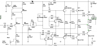
R18 has 10.7mv. Idle current is 48.7ma in each output device. This should be ok for the MJL21193/4.
C10 raised to 220n in the emulator. I think my working boards had 100n across the idle servo. Layout is good and very stable.
How do you feel about the choice of MJE15034/5 as drivers? They are TO220. I don't think a BD139/140 would drive 2 pair MJE21193/4.
R13 will have a trimmer in series with it before I do a PCB layout. For simulation, I try to use as few variables as possible to avoid confusing myself or getting lost.
R18 has 10.7mv. Idle current is 48.7ma in each output device. This should be ok for the MJL21193/4.
C10 raised to 220n in the emulator. I think my working boards had 100n across the idle servo. Layout is good and very stable.
How do you feel about the choice of MJE15034/5 as drivers? They are TO220. I don't think a BD139/140 would drive 2 pair MJE21193/4.
Those output transistors are very stout and two pairs will have no problems with 45V rails driving 4 ohm speakers. Those 50W MJE's are also very robust and adequately heatsinked will be able to drive a lot of current into those outputs, which is essential, because one drawback of the MJL's is that their hFE isn't particularly wonderful.
In fact the hFE of those drivers isn't that great either, so the one real problem with this OPS is that it doesn't have a lot of current gain, particularly for the stated usage.
I generally bias the driver stage HOT and eliminate the speed up cap, C15, altogether, although your arrangement is probably more conventional.
I'd buffer the VA stage with something like a BD140, which increase the Zin of OPS and increase loop gain. Then the VA transistor, Q6, can be changed to something smaller, faster and generally more suitable such as a KSC1845 running at about 2-3mA and bootstrapped to the VAS buffer with a 220 or 330 ohm resistor.
You absolutely need a zobel on the output and probably also the usual output inductor. I hardly ever both with the inductor but its best to include it if unsure. You probably want some HF rail decoupling caps.
All-in-all this is a very conventional and straight-forward design.
Those output transistors are very stout and two pairs will have no problems with 45V rails driving 4 ohm speakers. Those 50W MJE's are also very robust and adequately heatsinked will be able to drive a lot of current into those outputs, which is essential, because one drawback of the MJL's is that their hFE isn't particularly wonderful.
In fact the hFE of those drivers isn't that great either, so the one real problem with this OPS is that it doesn't have a lot of current gain, particularly for the stated usage.
I generally bias the driver stage HOT and eliminate the speed up cap, C15, altogether, although your arrangement is probably more conventional.
I'd buffer the VA stage with something like a BD140, which increase the Zin of OPS and increase loop gain. Then the VA transistor, Q6, can be changed to something smaller, faster and generally more suitable such as a KSC1845 running at about 2-3mA and bootstrapped to the VAS buffer with a 220 or 330 ohm resistor.
You absolutely need a zobel on the output and probably also the usual output inductor. I hardly ever both with the inductor but its best to include it if unsure. You probably want some HF rail decoupling caps.
All-in-all this is a very conventional and straight-forward design.
That was my next worry was if the VAS would provide enough current. Could a darlington be used in a VAS?
Something like this?
Attachments
Last edited:
The above modification did reduce distortion.
10hz 147w .025%
20hz 148.8w .025%
100hz 150w .025%
1khz 150w .026%
10khz 149w .041%
20khz 144w .054%
30khz 137.5w .098%
EDIT - Those numbers are wrong. I forgot to re-balance the LTP. Here are the correct figures.
10hz 150.8w .029%
100hz 150.9w .029%
1khz 150.9w .029%
10khz 149.4w .029%
20khz 145.1w .028%
30khz 138.5w .031%
Last edited:
Member
Joined 2009
Paid Member
How do you like the sound and performance? Which drivers did you use? Schematic available?
I've only run it briefly and I liked what I heard. I have previously built a clone of the lower power AKSA, many years ago and like that one too.
I ended up using TO-126 footprint drivers because my pcb layout had it baked-in. That was not my original intention - I have the AKSA drivers and was going to use them but used the wrong footprint. I did a bit of research on TO-126 drivers and after comparing different spec. sheets and reading all the recommendations on this forum I decided on the KSC2690 / KSA1220 pair available from DigiKey.
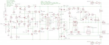
The schematic I used is essentially the AKSA 100W power amp. However, I find that I like to have dc-speaker protection built-in so my design includes that onto the pcb. It not only provides dc-protection but a modest turn-on delay and quick speaker disconnect when powered-off. This additional circuitry makes the schematic look more complicated than the basic amplifier but it takes up relatively little space on the pcb.
My goal was the AKSA sound. There are many 'improvements' you can make to the circuit. The buffered (Darlington) VAS adds greatly to the open loop gain and will reduce distortion but it's no longer the AKSA (I do have the provision for an additional transistor on my pcb but do not use it for this reason). In the end, if you want something with very low distortion that sounds amazing then I'd point you in a different direction altogether (search for TGM8) but if you like the bootstrap AKSA then I'd say 'go for it'.
Attachments
Last edited:
Member
Joined 2009
Paid Member
small correction - I ended up using a 10uf cap for C1 (not 22uF) and 2k2 from R9 (not 2k7) and I think I have 3A fuses (instead of 5A).
You mean R8?
What is C6 for?
Thanks for the schematic. I'll have to look into those drivers but I think I'll be ok with the MJE15034/5.
I intended on using a couple UPC1237 protection boards off ebay. Sort of a quick and easy solution to that. What are the pros and cons of shunting the driver's base using a transistor and driving that with the voltage across the emitter resistor? Current limiting I guess.
Last edited:
Member
Joined 2009
Paid Member
yes R8You mean R8?
phase lead compensation, works in concert with C5 allowing more stability with lower values of C5 - you can try different values of C5 to suit your ears over a range of about 30pF to 100pF. I liked 47pF when using C0G capacitors. The AKSA uses silva-mica capacitors.What is C6 for?
Yes, that'll work fine but my solid-state relay is expected to perform more reliably: read here: http://www.diyaudio.com/forums/solid-state/120365-loudspeaker-relays.htmlI intended on using a couple UPC1237 protection boards off ebay. Sort of a quick and easy solution to that.
Speaker DC protection with relays
I believe it's more sophisticated than that, can help with clipping - not sure of the details myself and am probably getting confused with the Baker clamp. Did you know Mr. Baker also patented the Diamond Buffer.What are the pros and cons of shunting the driver's base using a transistor and driving that with the voltage across the emitter resistor? Current limiting I guess.
yes R8
phase lead compensation, works in concert with C5 allowing more stability with lower values of C5 - you can try different values of C5 to suit your ears over a range of about 30pF to 100pF. I liked 47pF when using C0G capacitors. The AKSA uses silva-mica capacitors.
Yes, that'll work fine but my solid-state relay is expected to perform more reliably: read here: http://www.diyaudio.com/forums/solid-state/120365-loudspeaker-relays.html
Speaker DC protection with relays
I believe it's more sophisticated than that, can help with clipping - not sure of the details myself and am probably getting confused with the Baker clamp. Did you know Mr. Baker also patented the Diamond Buffer.
Not sure who that is. That Diamond Buffer looks a lot like a multivibrator.

Member
Joined 2009
Paid Member
The above modification did reduce distortion.
The design already has low enough distortion in my opinion, for this topology, so better to focus on the practical things.
Referring to your most recently posted schematic:
R17,18,21 and 22 are fairly low, good for minimal distortion, but makes device matching more critical and thermal stability less robust. If you've done this before then no problem, but if not, I'd recommend starting with 0R47.
You could add the provision for base stopper resistors on the drivers (Q3 and Q4); I used 100R but you might do fine with half that.
The bias is set by R13? - you want to put a potentiometer in series with R13. Don't remove R13, just add a potentiometer of, say 500R max with 25 turns (sealed unit) and reduce R13 to 470R.
R8 needs to be at least a 1W rated resistor, it takes the brunt of the bootstrap swinging up and down. Where's your zobel (R + C) on the output and an output inductor ? (look at my schematic)
You could add the provision for emitter degeneration on the LTP devices, Q7 and Q8. Even if you don't want any degeneration you could put a low value resistor in there (e.g. 2R2) to allow you to at least measure the current through each device so you can see if they are roughly balanced.
You want an r.f. filter on the input, i.e. a small capacitor (e.g. 330pF ceramic C0G) from the base of Q7 to signal ground. In conjunction with R2 (which would be better at 1K) you have a low-pass filter to stop the local radio station appearing at the input and getting 'detected' by the diode that Q7 will represent.
I'm not sure about your VAS, look at some published designs. I suspect you want C6 to go from the base of Q6 to the collector of Q14 but I'm not confident about that as I've never used a buffer after the VAS, only before it. I would recommend you read up on 'beta enhanced VAS' which places the buffer before the VAS and wraps the Cdom capacitor around the combination.
You might also want a ground-lift resistor at the input - again, look at my schematic, I think it's labelled R2.
You have your phase lead compensation, C3 from the output of the power stage. Some folk say that allows r.f. into the feedback network (r.f. picked up by your long speaker cables). I don't know if that's a real issue, but I've also placed my phase lead feedback cap from the output of the VAS (either below or above the Vbe multiplier) rather than the from the output of the power devices.
I've read that two-transistor current sources can have stability challenges and to mitigate this you put a small cap (e.g. 33p) between their bases.
Last edited:
I'm not sure about your VAS, look at some published designs. I suspect you want C6 to go from the base of Q6 to the collector of Q14 but I'm not confident about that as I've never used a buffer after the VAS, only before it. I would recommend you read up on 'beta enhanced VAS' which places the buffer before the VAS and wraps the Cdom capacitor around the combination.
Hi Gareth, Cdom is fine as-is but its also possible to enclose the VAS buffer inside C6 as you describe, and doing so would probably improve distortion further. One thing to bear in mind is that the more transistors enclosed within Cdom, the worse the stability margins get. It won't be an issue doing what you describe, but if he also added a CM and VAS 'beta enhancer' then that would result in four transistors enclosed by Cdom and you end up having to compensate the compensation loop!
VAS beta enhancer reduces the load on the input stage and increases its gain, while this buffer reduces the loading effects on the OPS on the VA stage, increasing its gain somewhat. If you look at the datasheets for the transistors used in the OPS you'll see there isn't a lot of gain, particularly at high currents, which is why I suggested the buffer.
cheers
Member
Joined 2009
Paid Member
I thought Cdom was the biggest load on the LTP, especially as frequency increases. Does the beta-enhancer or the EF buffer help much with that?VAS beta enhancer reduces the load on the input stage
That's right; however, while Cdom is (or should be!) a very linear capacitor, there is also the intrinsic collector-base junction capacitance of the VA transistor that presents a highly non-linear load to the LTP. The beta enhancer reduces the effect of this small 'C' load on the input stage by approx. its hFE. Since the beta enhancer's collector is tied to ground (or the opposite rail) its own C-B junction capacitance is not modulated with signal thus doesn't contribute to this problem. This is all explained far better and in more detail in Doug's book and possibly Bob's also.
Member
Joined 2009
Paid Member
I don't worry too much about the non-linearity of the C-B junction. The fact that it is non-linear doesn't increase the load on the LTP. And because it is inside the local VAS-only feedback loop created by Cdom I suspect that it gets linearized somewhat. Furthermore, we tend to pick low Cob transistors for the VAS device, so the non-linearity is swamped by the pcb parasitic capacitance and high-quality Cdom device, by at least a factor of 10. And I think it helps that the VAS is operated in Class A.... Well, to be honest, it's all theory to me and I could probably 'argue' both sides of the house to suit my mood - I'm a rank amateur when it comes to building amps !
Doug Self discusses the improvement afforded by the EF Buffer in much more detail in his 6th edition than in his earlier and online texts. Its worth buying a copy just for the analysis in this updated chapter. He provides the measurements from his AP and suffice to say the measured improvement is huge for the cost of a TO-92 and a resistor. Admittedly there are better suited VA transistors than the one he used, but its hard to imagine an amp with a good VA transistor wouldn't measure better with the EF added. We can argue whether the lower distortion matters from a subjective POV (I happen to agree the simple VAS is just fine most of the time) but objectively, the analysis is pretty conclusive.
I never understood why Self suggested the beta enhanced VAS was superior. It does unload the input stage, no question, and he points out that the loop gain is increased around 6dB. OTOH the 'helper EF' should have a resistor in collector to ground to ensure it does not blow up if things go south, and I have always had much more success with a CFP VAS; the npn master runs at 1mA and the slave at 8mA. This gives very high input impedance, same as the enhanced VAS, and very low output at the emitter of the pnp, which is a convenient point to string the base npn Cdom to the emitter pnp. I have always regarded as a high impedance output, as we see with the conventional VAS, as flawed; particularly when driving a Class AB output stage where at the crossover disjunction there are some very weird happenings. I would prefer a low impedance drive at this point rather than relying entirely on the negative feedback path.
HD
HD
Hi Hugh, what you've written makes sense to me, the only possible issue I see is that the IPS still has to drive the non-linear Cbc in the npn master, which was a major source of HF distortion, according to Self's analysis. It should be possible to put an EF buffer in front of the "CFP" VAS, although I've never tried this nor seen it done before. All these junctions are going to reduce the swing on the -ve rail, albeit only marginally.
Member
Joined 2009
Paid Member
at dc, but at 20kHz doesn't the LTP still faces the full wrath of Cdom ????It does unload the input stage
Last edited:
Yes, Gareth, BUT isn't the LTP seeing the dominance of the resistor between base and rail at audio?
At 1MHz, the impedance of a 33pF Cdom is 480R, same order as a 680R base/emitter resistor on a VAS...... At 20KHz the impedance of 33pF is higher, at 24k.
And I always felt that the Cdom more affected the OLG of the VAS itself rather than working on the LTP, Schaade fb if you will. LTP is important, but it's not strictly a VAS, it's a transconductance stage, voltage in to current out (with some reservations, some say a bipolar is driven by voltage not current, in truth it's driven by both.)
Hugh
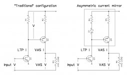
Hi Hugh, Gareth, Christian and All -
A few thoughts on the topic, if I may.
This is not something really new, however ... many designers don't use this approach.
Consider Q1, Q3 are part of LTP (can be singleton as well); Q2, Q4 are VAS transistors. R3, R6 are the VAS load equivalents (can be CCS, 2-nd push-pull shoulder, bootstrapped load, etc.).
Picture on the left - let say, traditional approach.
1) V-to-I in Q1 (non-linearity),
2) I-to-V on R1 (complex load - Cdom),
3) V-to-I in Q2 (non-linearity),
4) I-to-V on VAS load (good enough).
Two transconductance stages.
Miller capacitor is normal compensation approach in this case.
Picture on the right - current mirror as LTP load.
1) V-to-I in Q1 (non-linearity, same as before),
2) I-to-I with scaling (good enough, Cdom is not an issue any more),
3) I-to-V on VAS load (good enough).
Single transconductance stage.
This one is what I call "current drive" for myself (just one of its variants).
The only difference is D1, but now you can consider D1, Q4, R4, R5 as a single "building block" - a current mirror.
It can be improved further on - Wilson mirror, cascoded VAS output, allowing good matched small signal transistors in the mirror, etc.
This approach does not require miller capacitor - a small shunt cap in parallel with VAS load is enough for unconditional stability of the whole thing.
Overall result - better linearity and wider open loop bandwidth at the same time. As a "side effect" - all "current drive" designs are much less sensitive to external EMF, they are simply "more quiet" - just a practical observation.
What do you think?
Cheers,
Valery
Attachments
- Status
- This old topic is closed. If you want to reopen this topic, contact a moderator using the "Report Post" button.
- Home
- Amplifiers
- Solid State
- Bootstrapped amps. DX/Aksa/RCA/etc...