Assuming ideal transistors and ignoring base current errors, the voltage at the output of the diamond buffer (DB) emitter must equal the non-inverting input voltage. There is no voltage gain in the 1st stage of a CFA - all the voltage gain is in the 2nd stage which simply drives the feedback network so that the voltage at the emmitter of the DB output equals the input voltage. The output from the DB collector is the current delivered over and above that required from the feedback resistor to make the inverting input equal the non-inverting input. So (ignoring base current errors) the DB output transistor collector current is a copy of the current supplied into Rg minus the current supplied by the feedback resistor Rf.
Under steady state DC operating conditions and LF, the [change in] DB collector output current is very low (uA) since the TIS/TAS gain is high (50 to 60 dB in a jelly bean CFA) so little drive is required to maintain the output voltage to support the correct feedback voltages so that the two inputs are equal.
The current on demand action only comes into play when a fast signal (i.e. HF signal) is encountered. Here, the 2nd stage will simply drive the output as hard as necessary to ensure the inverting input equals the non-inverting input in order to charge up any capacitance (parasitic or compensation) around the second stage. In sims, you can feed a fast rise time signal input the input, and the DB collector current (which is driving the comp network around the 2nd stage) will 'spike' at 5-8x the standing current. So, as the input signal frequency is increased, the delta output current from the DB collector increases in magnitude. This is the 'current on demand' behaviour' and as a result, the amplifier bandwidth does not change with closed loop gain like a classic VFA. (But, it should be noted, this only applies over a fairly narrow 'sweet spot').
(I know some people will say 'ah you see a CFA is just a VFA because you've been talking about voltages' but its not - you are directly subtracting currents at the DB inverting input (unlike a VFA where you subtract voltages and steer the LTP current source into or away from the TIS input) and the error current is appearing at the DB collector output. )
I understand that and it makes sense.
I just read again the section on page 213 in Bob's 2nd Ed., using his fig 9.18.
"Notice that the value of R1 (=Rg, 100R) plays no role in affecting the loop gain if the output impedance of the input buffer is ideally zero (Here it is illustrated as 5R, so 95% of the current through R2 (=Rf, 2.7k) flows through the buffer" (between brackets mine).
So what does Rg do then??
Jan
Bonsai, look here, my super VFA
Ultra high speed VFA 500V/us
CFA like behavior, current on demand ...
What do you think ?
Ultra high speed VFA 500V/us
CFA like behavior, current on demand ...
What do you think ?
The current on demand action only comes into play when a fast signal (i.e. HF signal) is encountered. Here, the 2nd stage will simply drive the output as hard as necessary to ensure the inverting input equals the non-inverting input in order to charge up any capacitance (parasitic or compensation) around the second stage. In sims, you can feed a fast rise time signal input the input, and the DB collector current (which is driving the comp network around the 2nd stage) will 'spike' at 5-8x the standing current. So, as the input signal frequency is increased, the delta output current from the DB collector increases in magnitude. This is the 'current on demand' behaviour' and as a result, the amplifier bandwidth does not change with closed loop gain like a classic VFA. (But, it should be noted, this only applies over a fairly narrow 'sweet spot').
This is mostly an incorrect description; there is no relationship between the "current on demand" property (which is a large signal effect/property) and the bandwidth independent gain (which is a small signal effect/property).
The bandwidth independent gain effect/property relies causally on the (small signal) modulation of the loop gain (open loop gain, too) by the feedback resistor.
I understand that and it makes sense.
I just read again the section on page 213 in Bob's 2nd Ed., using his fig 9.18.
"Notice that the value of R1 (=Rg, 100R) plays no role in affecting the loop gain if the output impedance of the input buffer is ideally zero (Here it is illustrated as 5R, so 95% of the current through R2 (=Rf, 2.7k) flows through the buffer" (between brackets mine).
So what does Rg do then??
Jan
Because the input buffer is unity gain with low output impedance, the input signal voltage must appear across Rg. This creates a current flow in Rg in accordance with the input signal. Because virtually no signal current must flow through the buffer to the VAS input, due to high VAS gain, the current flowing through the feedback resistor must nearly equal that flowing through RG due to the input signal. That process forces the output signal to be that which, when divided by the feedback network consisting of the feedback resistor and shunt resistor Rg, is the same as the input voltage signal appearing at the output of the input buffer.
If the input signal is 1 V and the feedback divider is 10:1, then the output voltage will be 10V and the voltage at the output of the input buffer will be 1 volt, so that we are in equilibrium and no signal current need flow through the input buffer to keep the output of the buffer at a signal voltage of 1 V.
Any signal current that flows in the input buffer output is an error current.
Cheers,
Bob
Bonsai, look here, my super VFA
Ultra high speed VFA 500V/us
CFA like behavior, current on demand ...
What do you think ?
Are you sure you are not confusing the rise time with slewing rate? 80nS rise time (as stated) maps to a bandwidth of 3.5MHz, this is no indication for the amplifier slew rate. By no means can the 2mA tail current in your schematic charge the input stage output capacitance cap in 80nS, that would require a much higher tail current. With 2mA you can only charge a 4pF cap to 40V in 80nS, your PCB will have more than that (and that's even before considering Cb'c, etc...).
P.S. The MIC compensation (yours resembles that) can lead, in certain circumstances, to a "no slewing" result, meaning the amplifier never enters into slew rate limitations, see Bob's error correction amplifier (with the same 2mA current he reported (if memory serves) only 300V/uS slew rate). But this still doesn't support your "550V/uS" slew rate number, that's once again likely the effect of the amplifier wide bandwidth. BTW, the Stochino amp slews (real slew rate) so fast because of the very nice idea of current dumping from the cap placed between the two input stages halves (could be actually larger than 1nF). That cap dumps the extra current required to fast charge the compensation cap.
Last edited:
Because the input buffer is unity gain with low output impedance, the input signal voltage must appear across Rg. This creates a current flow in Rg in accordance with the input signal. Because virtually no signal current must flow through the buffer to the VAS input, due to high VAS gain, the current flowing through the feedback resistor must nearly equal that flowing through RG due to the input signal. That process forces the output signal to be that which, when divided by the feedback network consisting of the feedback resistor and shunt resistor Rg, is the same as the input voltage signal appearing at the output of the input buffer.
If the input signal is 1 V and the feedback divider is 10:1, then the output voltage will be 10V and the voltage at the output of the input buffer will be 1 volt, so that we are in equilibrium and no signal current need flow through the input buffer to keep the output of the buffer at a signal voltage of 1 V.
Any signal current that flows in the input buffer output is an error current.
Cheers,
Bob
So, there's really no chicken and egg issue. Input is switched on, buffer output rises, dumps current into Rg which is reflected through the mirrors into the output, far end on Rf rises, current starts to flow through Rf until it equals the current out of the buffer, at which point equilibrium is reached*.
Easy, really

Thanks Bob!
Jan
*Eqilibrium will of course not be reached fully as the OL gain is finite, so a very small current will remain to flow from the buffer to support the current the mirrors need to support the output signal. What Bob calls the error current.
Last edited:
So, there's really no chicken and egg issue. Input is switched on, buffer output rises, dumps current into Rg which is reflected through the mirrors into the output, far end on Rf rises, current starts to flow through Rf until it equals the current out of the buffer, at which point equilibrium is reached*.
Easy, really
Thanks Bob!
Jan
*Eqilibrium will of course not be reached fully as the OL gain is finite, so a very small current will remain to flow from the buffer to support the current the mirrors need to support the output signal. What Bob calls the error current.
Correct!
BTW, the classic 3-transistor phono preamp can be considered to be a CFA, in my opinion, since FB goes to the emitter of the first transistor, and that transistor can be thought of as an emitter follower buffer insofar as signal flow to its emitter. However, since the RIAA EQ acts by changing the value of the FB impedance with frequency, the loop gain in the RIAA phono preamp is a function of gain and frequency.
Note also that a 2-transistor CFP with gain is also a CFA circuit.
Cheers,
Bob
Are you sure you are not confusing the rise time with slewing rate? 80nS rise time (as stated) maps to a bandwidth of 3.5MHz, this is no indication for the amplifier slew rate. By no means can the 2mA tail current in your schematic charge the input stage output capacitance cap in 80nS, that would require a much higher tail current. With 2mA you can only charge a 4pF cap to 40V in 80nS, your PCB will have more than that (and that's even before considering Cb'c, etc...).
P.S. The MIC compensation (yours resembles that) can lead, in certain circumstances, to a "no slewing" result, meaning the amplifier never enters into slew rate limitations, see Bob's error correction amplifier (with the same 2mA current he reported (if memory serves) only 300V/uS slew rate). But this still doesn't support your "550V/uS" slew rate number, that's once again likely the effect of the amplifier wide bandwidth. BTW, the Stochino amp slews (real slew rate) so fast because of the very nice idea of current dumping from the cap placed between the two input stages halves (could be actually larger than 1nF). That cap dumps the extra current required to fast charge the compensation cap.
yes, I am quite sure
a simulation file is here , try it, you will see
Ultra high speed VFA 500V/us
I don't have real amp, just simulation
Move the CFA discussion
I think it is time to move the CFA discussion from this thread to the CFA thread. This is a potentially toxic discussion that provides little insight that was not already discussed in the other thread. Of course, if anyone finds an error in my CFA discussion in my book, that is fair game here.
Cheers,
Bob
I don't have real amp, just simulation
Ok, simulation only, no parasitic elements considered. Since I am not a LTSpice user, I can't reproduce.
Are you sure the amp is entering the slew rate limit at 550V/uS, that is, the input stage saturates? If it doesn't, then your model is non slewing and the 550V/uS is actually a non constant (amplitude dependent) result of the rise/fall times.
P.S. I am not nitpicking; it's an important distinction, since slewing limitation creates distortions, while a finite rise/fall time does not.
Last edited:
I think it is time to move the CFA discussion from this thread to the CFA thread.
Link to the thread for those looking: CFA Topology Audio Amplifiers
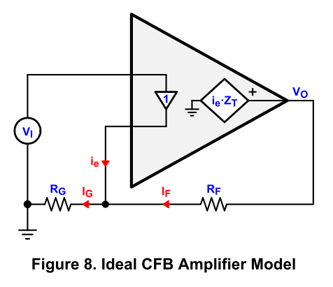
Assuming this is the major trap in analysing how an input stage works.Assuming ideal transistors and ignoring base current errors, the voltage at the output of the diamond buffer (DB) emitter must equal the non-inverting input voltage.
Refering to Renesas figure below :I know some people will say 'ah you see a CFA is just a VFA because you've been talking about voltages' but its not - you are directly subtracting currents at the DB inverting input
Ig = Ie + If
You interpret this as :
Ie = Ig - If
Ie being almost equal to Ic delivered by the input stage.
But Ie is not determined by this difference of currents between Ig and If.
Ie is determine by the voltage between the non inverting input and the inverting input. Otherwise said, it is under the control of Vbes of the input stage.
You see, it is just a VFA.
In the name of some people.
Last edited:
"The bandwidth independent gain effect/property relies causally on the (small signal) modulation of the loop gain (open loop gain, too) by the feedback resistor. "
Are you referring here to the small signal DB gm changes?
I mean, changing the closed loop gain, by changing the feedback network resistor (within small closed loop gain limits), also changes the amp open loop gain, so that the bandwidth and closed loop gain are no longer related through the GBW. This is a small signal mechanism, nothing to do with "current on demand".
In a VFA, changing the closed loop gain does not change the amp open loop gain, therefore the GBW constraint holds.
That's the view I began to defend with this post in november 2018 :So, there's really no chicken and egg issue. Input is switched on, buffer output rises, dumps current into Rg which is reflected through the mirrors into the output, far end on Rf rises, current starts to flow through Rf until it equals the current out of the buffer, at which point equilibrium is reached.
https://www.diyaudio.com/forums/sol...dback-amplifiers-semantic-35.html#post5597832
I created the thread, it was tumultuous.
Last edited:
I mean, changing the closed loop gain, by changing the feedback network resistor (within small closed loop gain limits), also changes the amp open loop gain, so that the bandwidth and closed loop gain are no longer related through the GBW. This is a small signal mechanism, nothing to do with "current on demand".
In a VFA, changing the closed loop gain does not change the amp open loop gain, therefore the GBW constraint holds.
Why would you change the feedback resistor in a CFA? You optimize it for overshoot or phase margin (whatever you choose) and then adjust Rg to set the correct gain. The gm is set by the feedback resistor in a CFA (unlike a VFA).
On a VFA, pole splitting aka dominant pole compensation means the OLG drops off at 20 dB/decade. On a CFA (unless it’s high OLG as mentioned in an earlier post) you don’t have to apply pole splitting so you get more bandwidth available.
But, I think the suggestion from Bob that we take this elsewhere for discussion is a good one.
Assuming this is the major trap in analysing how an input stage works.
Refering to Renesas figure below :
Ig = Ie + If
You interpret this as :
Ie = Ig - If
Ie being almost equal to Ic delivered by the input stage.
But Ie is not determined by this difference of currents between Ig and If.
Ie is determine by the voltage between the non inverting input and the inverting input. Otherwise said, it is under the control of Vbes of the input stage.
You see, it is just a VFA.
In the name of some people.
I am not going to get into a discussion with you on this forr. With all due respects, it will go precisely nowhere. You’ve had luminaries like Scott try to explain this you and you still persist.
Apologies in advance for being so blunt.
I will step away from this specific subject on this thread now.
Last edited:
- Home
- Amplifiers
- Solid State
- Bob Cordell's Power amplifier book