The Bilotti paper suggests that the quantity of interest is the ratio between the emitter degeneration resistance and the base spreading resistance. Since base spreading resistance varies (enormously) between device types, perhaps the recommended optimum design point also varies (enormously) between device types. Perhaps the right way to design a current mirror when using 2N4401s (rbb = 40) is not the right way to design a current mirror when using BD437s (rbb=3.9).
Bob, I don't understand this - I would have thought that the mirror degeneration resistor might be too high for low noise?
Jan
Hi Jan,
Yes, this is definitely non-intuitive. The problem is not the thermal noise of the degeneration resistors in the current mirror. The source of the noise is the transistors themselves - their shot noise which translates to an effective input-referred noise when those transistors are viewed as common-emitter stages. That input-referred noise of those transistors is impressed across the degeneration resistors, resulting in noise current that pollutes the signal current coming out of the input pair. The smaller the value of the emitter degeneration resistor, the larger is that noise current. This is a good example of why simulation is so important in noise analysis.
BTW, for a given amount of noise current emanating from the current mirror, the lower the transconductance of the LTP, the worse is the input-referred noise contribution.
In a resistively-loaded VAS, one is dealing with the thermal noise of the load resistor and the input current noise of the VAS. One also needs to evaluate the effective voltage gain of the input stage, which sometimes can be surprisingly low. If it is on the low side, the final input-referred contribution of the usually-noisier VAS will not be swamped out by the gain, and this noise will be a contributor that cannot be ignored.
Noise analysis of folded cascode IPS-VAS must also be done diligently, recognizing that now the VAS output signal current is no greater than the output signal current of the IPS. Also, the noise contribution of the combination of the cascode bias resistor-cascode transistor must be considered (similar issue to the current mirror emitter resistor issue).
Cheers,
Bob
Mr. Cordell is right this time. In a current source, the emitter degeneration component of the collector noise current is inverse proportional to the square root of the emitter degeneration resistor value. Perhaps counter intuitive, but that's it.
Grab a pen and calculate; you'll find that the collector noise current is about the emitter degeneration resistor noise voltage divided by the emitter degeneration resistor. Since the emitter degeneration resistor noise voltage is proportional to the square root of the resistor value, it follows that the collector noise current is proportional to the square root of the emitter degeneration resistor value.
Perhaps more intuitive, it happens because the emitter degeneration resistor noise voltage is divided by the resistor and the transistor rb'e. The larger the emitter degeneration resistor, the smaller the transistor "input" voltage, but since the resistor noise increases only as sqrt with the resistor value, increasing the resistor actually decreases the output noise current.
What? Right only this time? Just kidding.
You have correctly analyzed the contribution of the thermal noise of the emitter degeneration resistor. However, I don't think you took into account the contribution of the transistor's shot noise and base spreading resistance noise. These are effectively voltage noise sources at the base of the transistor. Their contribution to output noise current is in direct proportion to the net transconductance of that transistor as degenerated by Re (which is 1/(re+Re)). This contribution will often dominate.
Cheers,
Bob
Mr. Cordell is right this time. In a current source, the emitter degeneration component of the collector noise current is inverse proportional to the square root of the emitter degeneration resistor value. Perhaps counter intuitive, but that's it.
Grab a pen and calculate; you'll find that the collector noise current is about the emitter degeneration resistor noise voltage divided by the emitter degeneration resistor. Since the emitter degeneration resistor noise voltage is proportional to the square root of the resistor value, it follows that the collector noise current is proportional to the square root of the emitter degeneration resistor value.
Perhaps more intuitive, it happens because the emitter degeneration resistor noise voltage is divided by the resistor and the transistor rb'e. The larger the emitter degeneration resistor, the smaller the transistor "input" voltage, but since the resistor noise increases only as sqrt with the resistor value, increasing the resistor actually decreases the output noise current.
What about rb'e. Is a greater rb'e desirable?
The problem is not the thermal noise of the degeneration resistors in the current mirror. The source of the noise is the transistors themselves - their shot noise which translates to an effective input-referred noise when those transistors are viewed as common-emitter stages. That input-referred noise of those transistors is impressed across the degeneration resistors, resulting in noise current that pollutes the signal current coming out of the input pair. The smaller the value of the emitter degeneration resistor, the larger is that noise current.
I believe this is, in general, and for the common low noise devices, incorrect.
For both noise sources, Rbb' (the base spreading resistance) and the degeneration resistor, the collector noise current transconductance gain is the same, approximately the inverse of the degeneration resistor 1/Re (for common bias conditions, large beta, etc...). The Re voltage noise itself is proportional to SQRT(Re), so its collector current noise contribution is proportional to 1/SQRT(Re), so it decreases with Re. The Rbb' voltage noise is proportional to SQRT(Rbb'), so its collector current noise contribution is proportional to SQRT(Rbb')/Re, so it also decreases with increasing Re.
At least for low noise devices (where this kind of analysis makes sense), Rbb'<<Re so it's the emitter degeneration resistor that has a larger contribution to the collector noise current.
The current mirror current noise adds with the gain stage current noise and both flow into the stage load. The total current noise multiplied by the load impedance Zload is the output noise voltage, which divided by the 2*gm*Zload (the stage voltage gain) leads to the input referred noise. If the gain stage has the same degeneration as the current mirror (a particular case, of course), then the input referred voltage noise is proportional to 1/(gm*SQRT(Re)) so it decreases with increasing Re as well. I don't think there is any noise optimum in the degeneration resistor, always the larger the better, but of course a large degeneration eats up headroom.
Very hard to explain without algebra, I suppose I did a crap job above, this is textbook stuff though, Motchenbacher and Fitchen has the whole derivation and discussion in detail. Simulation may help, but most of the bipolar models are not intended to model the noise, they usually have a Rbb' value either set to zero (the default) or very small.
What Mr. Cordell is saying may hold for very small degeneration resistors (like Re=10ohm) and rather noisy devices (say with Rbb'=100ohm). Then the whole model flips, since Rbb'>>Re. Then indeed the Rbb' noise dominates the input referred voltage noise.
Finally, it should be mentioned that a current source/current mirror always has more noise than a simple load resistor. Of course, the simple load resistor has zero PSRR, etc...
Last edited:
What about rb'e. Is a greater rb'e desirable?
Rb'e, you don't have direct control over that, its Beta/gm, gm depends on the DC collector current, which is, for a current mirror, an external variable.
Rb'e is a model only (doesn't exist physically) and as such it is not considered a noise source (Johnson or excess).
What? Right only this time? Just kidding.
You have correctly analyzed the contribution of the thermal noise of the emitter degeneration resistor. However, I don't think you took into account the contribution of the transistor's shot noise and base spreading resistance noise. These are effectively voltage noise sources at the base of the transistor. Their contribution to output noise current is in direct proportion to the net transconductance of that transistor as degenerated by Re (which is 1/(re+Re)). This contribution will often dominate.
Sorry this is, for the most common cases, not correct. The transistor base shot noise current SQRT(2*q*Ib)=SQRT(2*KT*gm/Beta) matters only at large collector currents, where gm is large. If you equal the shot noise to the Rbb' spreading resistance noise, you'll find that the collector current has to be 2*Vt*Beta/Rbb'. For a device with Rbb'=100ohm and beta 100 Ic has to be 56 mA so the shot noise equals the spreading resistance noise. True low noise bipolars have a base spreading resistance of a very few ohm, so the collector current is in the hundreds of mA (to have an equal contribution compared to Rbb'). Not the common usual case for an input stage.
This confirms what I just said, for low noise devices and the common biases in an input stage Rbb' noise dominates by far.
Thanks for the opportunity of recalling these bipolar things, I'm so sick of the mosfet noise crap from my daily job.
Last edited:
Waly, you're mixing your upper and lower case notation up, makes it hard to follow. Re is extrinsic emitter resistance a parasitic for me (often quite small), re is the term proportional to Ic. I'm also used to seeing rbb' as the base spreading resistance not Rbb'.
Yes, I messed up the notations. The degeneration should be RE, Re is for the emitter extrinsic resistance. Rbb' should be rbb', Rb'e should be rb'e. Add to these the browser desire to correct the spelling and you got the whole mess.
It's almost impossible to put these calculations on a text only forum, but, as I said, this is text book stuff, at least it was taught at our university at the graduate level.
Enough for today...
Last edited:
Finally, it should be mentioned that a current source/current mirror always has more noise than a simple load resistor. Of course, the simple load resistor has zero PSRR, etc...
Finally we get there. Why in low noise preamps JC uses low value resistor only. and deals with the other issues in different way.
Thx-RNMarsh
I believe this is, in general, and for the common low noise devices, incorrect.
For both noise sources, Rbb' (the base spreading resistance) and the degeneration resistor, the collector noise current transconductance gain is the same, approximately the inverse of the degeneration resistor 1/Re (for common bias conditions, large beta, etc...). The Re voltage noise itself is proportional to SQRT(Re), so its collector current noise contribution is proportional to 1/SQRT(Re), so it decreases with Re. The Rbb' voltage noise is proportional to SQRT(Rbb'), so its collector current noise contribution is proportional to SQRT(Rbb')/Re, so it also decreases with increasing Re.
At least for low noise devices (where this kind of analysis makes sense), Rbb'<<Re so it's the emitter degeneration resistor that has a larger contribution to the collector noise current.
The current mirror current noise adds with the gain stage current noise and both flow into the stage load. The total current noise multiplied by the load impedance Zload is the output noise voltage, which divided by the 2*gm*Zload (the stage voltage gain) leads to the input referred noise. If the gain stage has the same degeneration as the current mirror (a particular case, of course), then the input referred voltage noise is proportional to 1/(gm*SQRT(Re)) so it decreases with increasing Re as well. I don't think there is any noise optimum in the degeneration resistor, always the larger the better, but of course a large degeneration eats up headroom.
Very hard to explain without algebra, I suppose I did a crap job above, this is textbook stuff though, Motchenbacher and Fitchen has the whole derivation and discussion in detail. Simulation may help, but most of the bipolar models are not intended to model the noise, they usually have a Rbb' value either set to zero (the default) or very small.
What Mr. Cordell is saying may hold for very small degeneration resistors (like Re=10ohm) and rather noisy devices (say with Rbb'=100ohm). Then the whole model flips, since Rbb'>>Re. Then indeed the Rbb' noise dominates the input referred voltage noise.
Finally, it should be mentioned that a current source/current mirror always has more noise than a simple load resistor. Of course, the simple load resistor has zero PSRR, etc...
We are both in violent agreement that larger emitter degeneration resistors in the current mirror will yield a lower noise contribution to current noise by the current mirror. However, as I pointed out, the thermal noise contribution of the emitter degeneration resistor is only one component, and you correctly pointed out the square root relationship in its contribution.
But there is another component. There is an equivalent voltage noise contributor that can be modeled as a noise voltage source at the base of the current mirror transistor. The effect of this noise source on output noise current of the current mirror goes directly as the inverse of the value of the degeneration resistor, RE (assuming RE >> re' for simplicity).
This holds true even for an ideal transistor without any ohmic base or emitter resistance. The equivalent input voltage noise of such a transistor, as you know, is numerically equal to the thermal noise of a resistor whose value is half of 1/gm. For a transistor operating at 1mA, 1/gm is about 26 ohms, and half of that is 13 ohms. The apparent input voltage noise of that transistor, which is its shot noise, is thus equal numerically to the thermal noise of a 13-ohm resistor. As you know, equivalent input-referred voltage noise of an ideal transistor is equal to the shot noise current divided by the transconductance. That being a voltage noise, it increases directly as the value of the emitter degeneration resistor value plus re' decreases. In the limit, as the degeneration resistor value becomes much larger than 1/gm, the current noise contribution due to shot noise goes up directly as the value of the degeneration resistor goes down. If the degeneration resistor drops 1 Vbe, its value will be about 10X that of 1/gm.
I think if you do a few simulations, the way in which these two noise contributors change with the value of the emitter degeneration resistor will become clear. Build a current mirror and start with 1 Vbe of degeneration and look at the output noise current. Now quadruple the amount of degeneration to 4 Vbe, all else held the same. According to your view, the output noise current will be cut in half. If According to my view, where one noise source goes as the square root and the other goes almost directly, you will see the output noise go down by more than a factor of 2.
As a further sanity check, do the same experiment with a 1k resistor in series with each base of the current mirror, emulating a transistor with very high base resistance, and contributing about 4.2 nV/rt Hz. Do this with a high-beta transistor to minimize the contribution of base current noise. In this experiment, you will see the output noise go down by closer to a factor of 4.
Cheers,
Bob
We are both in violent agreement that ...
Those who make peaceful agreement impossible will make violent agreement inevitable. - Not John F. Kennedy.
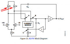
Finally we have the opportunity to ask ourselves: why does the world's lowest noise device (AD797) use current source loads on the input stage, rather than resistor loads? Are resistor loads STUPID?
Opamps have to play nice with realistic PSRR and voltage budgets.
")
Finally we have the opportunity to ask ourselves: why does the world's lowest noise device (AD797) use current source loads on the input stage, rather than resistor loads? Are resistor loads STUPID?
emitter coupled folded cascode current mirror? Low Z at nodes A and B.
-RNM
Investigate the NE5534 and the LT1028 opamps. In both cases the input stage is an undegenerated NPN diffpair with resistor loads. OP27/37 too, but it was designed by the same guy who did the LT1028.Opamps have to play nice with realistic PSRR and voltage budgets.
LT1028 PSRR is 130dB, DC gain is 143dB, CMRR is 122dB, input common mode range is (|rail| - 3.3V), output swing is (|rail| - 2.3V). It doesn't appear to me that the resistor loaded input stage has produced unrealistic PSRR and voltage budgets.
Some people have succeeded in making ultra low noise opamps by using resistor loaded diff amp first stages, and others have succeeded by using current source loaded folded cascode single stage topologies. We have existence proofs that neither approach is impossible. Putting it another way, John Curl devotees are half right: resistor loads are one way, but not the only way, to get a low noise first stage.
JC knows that i am sure and made his choice based also on listening evaluations - from others many times. But then also he might not have published his best. designs, also.
and it is dangerous to use simplified diagrams on marketing spec sheets as the whole truth of the topolgy. might even be wrong.
THx-RNMarsh
and it is dangerous to use simplified diagrams on marketing spec sheets as the whole truth of the topolgy. might even be wrong.
THx-RNMarsh
it is dangerous to use simplified diagrams on marketing spec sheets as the whole truth of the topolgy. might even be wrong.
THx-RNMarsh
I was going to make the same point - we know that data sheet 'simplified diagrams' are just that - I often wonder what important details are left out to protect company IP.
Jan
Here is the (30 years old, can you believe it?!) ISSCC paper about the LT1028 low noise opamp. The bottom left paragraph on page 1 says
The input stage is resistively loaded (R1 through R6 in Figure 2),
and the noise of the resistors is 11nV / rtHz. The sum of the second
stage voltage noise and current noise flowing through the load resistors
also equals 11nV / rtHZ at 1kHz; i.e., even the second stage has to be
a relatively low noise amplifier by itself. When these noise sources are
attenuated by the input stage gain of 100, and is rms summed with the
input transistors' noise, the net increase in the total amplifier noise is
1.3%.
I don't think George Erdi is lying or simplifying; In my opinion this paragraph tells the truth, the whole truth, and nothing but the truth.and the noise of the resistors is 11nV / rtHz. The sum of the second
stage voltage noise and current noise flowing through the load resistors
also equals 11nV / rtHZ at 1kHz; i.e., even the second stage has to be
a relatively low noise amplifier by itself. When these noise sources are
attenuated by the input stage gain of 100, and is rms summed with the
input transistors' noise, the net increase in the total amplifier noise is
1.3%.
Attachments
- Home
- Amplifiers
- Solid State
- Bob Cordell's Power amplifier book