... virtually any amplifier infinite...open-loop gain with a very small amount of positive feedback...
I think this is one interpretation of the distortion cancellation of the AD797.
I believe you eventually accepted this viewpoint after some initial skepticism?
This looks beneficial in theory, does any other op-amp use this?
Why is it not more common? I assume there are stability concerns over parameter variation or similar issues?
Best wishes
David
I think it does. It is simply something that is not in the input signal, so feedback will reduce it, the more so, the more loop gain is available at that low frequency.
Reading Bob's very good post above I believe we should more emphasize the falling of distortion at lower frequencies, rather than thinking the high frequency distortion rises, which it doesn't.
Jan
OK Jan you are correct.
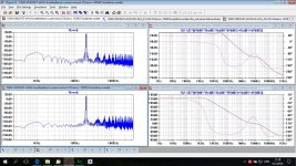
I simulated mine two CFAs, one with wide bandwidth of 80 dB of LG and the same amp, but now instead of simple resistor loaded IPS it is active loaded with CMs and it has not so wide bandwidth but with 120 dB LG up to 1kHz.
Damir
Attachments
I think this is one interpretation of the distortion cancellation of the AD797.
I believe you eventually accepted this viewpoint after some initial skepticism?
This looks beneficial in theory, does any other op-amp use this?
Why is it not more common? I assume there are stability concerns over parameter variation or similar issues?
Best wishes
David
Not quite it is only AC not the DC Aol. The feedback factor is tiny (only the error portion) so the effect on frequency response is minimal until you get to quite high in frequency. Once you are at a closed-loop gain of 20dB or so it can be ignored. One could say neutralization of the input capacitance in an RF amp is also a kind of positive feedback. That was the original analogy to try and differentiate it from an additional loop with gain like a CFP.
On the data sheet there are some applications where you can partially neutralize the comp cap from the same pin by going to ground rather than the output.
The benefits were published as well as the theory. The removal of the crossover "glitch" is shown pictorially.
As it turns out the flat 1nV of noise out to the full BW due to the single stage signal path was probably more of a benefit in applications outside of audio.
Last edited:
OK Jan you are correct.
I simulated mine two CFAs, one with wide bandwidth of 80 dB of LG and the same amp, but now instead of simple resistor loaded IPS it is active loaded with CMs and it has not so wide bandwidth but with 120 dB LG up to 1kHz.
Damir
John are you seeing this?
OK Jan you are correct.
I simulated mine two CFAs, one with wide bandwidth of 80 dB of LG and the same amp, but now instead of simple resistor loaded IPS it is active loaded with CMs and it has not so wide bandwidth but with 120 dB LG up to 1kHz.
Damir
JC usually needs low noise as well as low distortion. He uses low R values. Which is lowest noise... active load or resistor load?
THx-RNMarsh
JC usually needs low noise as well as low distortion. He uses low R values. Which is lowest noise... active load or resistor load?
THx-RNMarsh
Interesting question.
But John's designs are not really state of the art as far as distortion goes. Distortion clearly standing out of the noise. It s probably not wise to lower the noise further at the expense of increasing the distortion even more, which as Dadod showed is what would happen.
Jan
JC usually needs low noise as well as low distortion. He uses low R values. Which is lowest noise... active load or resistor load?
THx-RNMarsh
Look at the feedback network resistor values in the JC-1. They are fairly high, and are that way in part to achieve a balanced input. These higher value feedback resistors contribute significant thermal noise. The arrangement is much like that of a single op amp instrumentation amplifier. There are many power amplifiers out there with lower noise than the JC-1.
In a power amplifier, there are many more noise contributors in play at not-insignificant levels than just the input transistors or their associated emitter degeneration resistors. The impedance in the feedback network is one of them. The impedance in the input network is another one, easily overlooked, even when the amplifier input is shorted. The series resistor often present as part of the input LPF is also a contributor if you want a reasonably low input LPF cutoff frequency while not having an amplifier with high input capacitance. Just remember this rule of thumb: a 1k resistor creates 4.2 nV/rt Hz of thermal noise. But there are many others that come after the collectors of the input pair.
Further to your question about input stage load noise influences, I do go into this in a new noise chapter in my second edition. The answer depends a lot on the particular topology and component values, so I don't think one can make a hard-and-fast conclusion. But here is one example. In an input stage loaded with a current mirror, the value of the current mirror degeneration resistors is very important. In combination with the shot noise of the current mirror transistors, their value being to low can create enough noise to overwhelm the input-referred noise of the input LTP. Self often just puts 100 ohms in there, and that is usually too low. Yet, there is a tradeoff, since larger current mirror degeneration resistors can begin to eat into headroom. My recommendation is to never drop less than 1/2 Vbe across those resistors.
Because there are so many potential noise sources, some of whose contributions may not be obvious or at first intuitive, I believe it is imperative to do noise simulations if one is serious about confidently achieving optimally low noise. LTspice allows you to look at the relative contribution of every single contributor.
Cheers,
Bob
Bob, I don't understand this - I would have thought that the mirror degeneration resistor might be too high for low noise?
Jan
But here is one example. In an input stage loaded with a current mirror, the value of the current mirror degeneration resistors is very important. In combination with the shot noise of the current mirror transistors, their value being to low can create enough noise to overwhelm the input-referred noise of the input LTP.
Cheers,
Bob
Jan
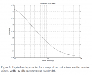
Jan, take a look at Samuel Groner's critique of D.Self's 5th edition, page 4, Figure 3. Groner built several "model amplifiers" (all TO92 IPS + VAS + classA_EF_OPS) and measured their equivalent input noise with different values of emitter degeneration resistors in the current mirror. What he found in real life, exactly matches what you and I see in LTSPICE ".NOISE" simulations: bigger degeneration resistances in the mirror, give lower noise. Groner realized that measured data on real amplifiers woulld be a LOT more convincing than simulations or equations, and that's what he did.Bob, I don't understand this - I would have thought that the mirror degeneration resistor might be too high for low noise?
This forced Self to add a couple of paragraphs to the 6th edition, not quite admitting that he made a design error, but instead marvelling over this discovery of a new noise source (6th edition p.152).
_
Attachments
Bob, I don't understand this - I would have thought that the mirror degeneration resistor might be too high for low noise?
Mr. Cordell is right this time. In a current source, the emitter degeneration component of the collector noise current is inverse proportional to the square root of the emitter degeneration resistor value. Perhaps counter intuitive, but that's it.
Grab a pen and calculate; you'll find that the collector noise current is about the emitter degeneration resistor noise voltage divided by the emitter degeneration resistor. Since the emitter degeneration resistor noise voltage is proportional to the square root of the resistor value, it follows that the collector noise current is proportional to the square root of the emitter degeneration resistor value.
Perhaps more intuitive, it happens because the emitter degeneration resistor noise voltage is divided by the resistor and the transistor rb'e. The larger the emitter degeneration resistor, the smaller the transistor "input" voltage, but since the resistor noise increases only as sqrt with the resistor value, increasing the resistor actually decreases the output noise current.
Wow...! Mark, Waly, I learned something gain. Indeed counter-intuitive.
Wasn't a Linear Audio short note touching this topic, in your very first volume? I got a copy from the author.
OK, I'll look it up tomorrow at my office.
Jan
The original...
Bilotti JSSC 75 June: Noise characteristics of current mirror | Analog Lib
Stating the result differently really gets a rise out of some folks. The result is a current with less than shot noise. I find it hard to believe some still get this wrong.
Last edited:
Longform versionThe original...
Attachments
Longform version
Thanks, I thought that site had a free download I've had a copy since 1975.
Jan, take a look at Samuel Groner's critique of D.Self's 5th edition, page 4, Figure 3. Groner built several "model amplifiers" (all TO92 IPS + VAS + classA_EF_OPS) and measured their equivalent input noise with different values of emitter degeneration resistors in the current mirror. What he found in real life, exactly matches what you and I see in LTSPICE ".NOISE" simulations: bigger degeneration resistances in the mirror, give lower noise. Groner realized that measured data on real amplifiers woulld be a LOT more convincing than simulations or equations, and that's what he did.
This forced Self to add a couple of paragraphs to the 6th edition, not quite admitting that he made a design error, but instead marvelling over this discovery of a new noise source (6th edition p.152).
_
Mark
I took a look at Samuels document, I found it on his home site.
It seems like he is only focusing on the value of the Emitter degeneration resistor in the current mirror to get the lowest noise.
In my opinion he should have looked at the voltagedrop across the Emitter degeneration resistor RE (AKA the feedback resistor in the CM). That is because the value of RE depends on the Collector current IC.
As I have posted earlier in this thread as an answer to a question from Edmond, I have found that a 5V voltagedrop across RE is a good compromise between noise and gain (low THD).
the same analysis is of course right for a Current source
http://www.diyaudio.com/forums/solid-state/171159-bob-cordells-power-amplifier-book-508.html#post4210071
Wally
I haven't read the note by Syn08 so I don't know if he was discussing this.
Cheers
S
- Home
- Amplifiers
- Solid State
- Bob Cordell's Power amplifier book