Input bias current cancellation is not much of an issue, since betas of the NPN and PNP pairs are not likely to be the same unless you get lucky. If they differed by a factor of 2, you would only get half cancellation. Also, note that several designers use a full complementary IPS implemented with JFETs, where input bias current cancellation is not an issue.
Cheers
Hi Bob,
D. Self in his book mentioned input distortion if input filter resistor is of higher value than 100 ohm(and we have to add the source output impedance). That distortion is coming from highly non linear input bias current. I think that this distortion can be much lover with symmetrical NPN/PNP input where we have some input bias current cancellation, what is quite common in a CFA where a complementary input pairs are used(beta matching) .
BR Damir
Another Member posted a link to test results for various manufacturers' 9240/9140 & 240/140.Hi Damir,
I'm sorry to be so slow in getting back to you. My wife has me looking for new carpeting, among a slew of other things. I have also been trying to finish my writeup of measurement results for resistor voltage-dependent distortion.
Its been awhile since I did those models, so I had to look up some old files to answer your question about the apparent reversal of Kp for the IRFP240 and IRFP9240 vertical MOSFETs. I believe those numbers are not reversed and are indeed correct. I realize it is non-intuitive for a P channel device to appear to have higher gm than an N channel device. However, I went back and even double-checked the IRF datasheets and it does appear that the IRFP9240 has greater gm than the IRFP240 at a given current. I re-simulated some of my device modeling SPICE test benches and it still seems to hang together.
Its been awhile, but I also seem to see that Kp by itself is not all there is to gm, and that the ratio of Kp of 2 devices in the model may not reflect the ratio of the gm of the 2 devices, both operating at the same drain current. Note that what is important is gm vs. Id.
Note also that tabular spec sheet numbers for minimum transconductance and not always all that useful, especially for evaluating SPICE models. I used actual IRF datasheet curves to make my models. I also did some lab measurements of individual devices.
I encourage others here to double check me on this. Errors are indeed possible and I always appreciate people pointing them out.
Cheers,
Bob
There does seem to be some evidence that some 9240/240 have got a swapped gm parameter when actually measured. This confirms your datasheet extractions.
But that did not hold for all manufacturers.
Thanks Mr. Cordell.Hi Alan,
Two things to keep in mind. First, the push-pull VAS gives twice the peak drive current to the output stage for a given idle current. So it has a dissipation advantage for the VAS transistor and is better at driving a 2 EF output stage, where output stage current gain is marginal, especially when there is beta droop in the output stage transistors at high current drive levels.
Also, symmetry in the VAS is desirable, and equal slew rate capability in both directions is a worthy goal (although slew rate is not always dictated by VAS current capability).
Cheers,
Bob
If symmetrical VAS is necessary, then it's easier to have complementary differential IPS.
My question is what is the disadvantage of VAS with CCS on one side if the CCS pull higher current to exceed the slew rate requirement? I agree that you'll get a little more even harmonics, but that might not be too bad as there are people that rave on SE tube amps that have higher 2nd harmonics.
Thanks
Hi Bob,
D. Self in his book mentioned input distortion if input filter resistor is of higher value than 100 ohm(and we have to add the source output impedance). That distortion is coming from highly non linear input bias current. I think that this distortion can be much lover with symmetrical NPN/PNP input where we have some input bias current cancellation, what is quite common in a CFA where a complementary input pairs are used(beta matching) .
BR Damir
Yet another reason to use a JFET input!
I would say that his comment may apply to only some IPS designs. Nevertheless, it underscores the need for us to do our amplifier simulations with some source resistance. Note that any such comment also applies to the other side of the LTP, namely the feedback network.
Any cancellation of static dc input bias current may not have any bearing on distortion.
Cheers,
Bob
Another Member posted a link to test results for various manufacturers' 9240/9140 & 240/140.
There does seem to be some evidence that some 9240/240 have got a swapped gm parameter when actually measured. This confirms your datasheet extractions.
But that did not hold for all manufacturers.
Good point. I based my models on the Id vs. Vgs transfer curves.
Cheers,
Bob
Yet another reason to use a JFET input!
I would say that his comment may apply to only some IPS designs. Nevertheless, it underscores the need for us to do our amplifier simulations with some source resistance. Note that any such comment also applies to the other side of the LTP, namely the feedback network.
Any cancellation of static dc input bias current may not have any bearing on distortion.
Cheers,
Bob
For my VFA amp with LTP I use a JFET, but for my CFA mosfet I use bipolars.
BR Damir
Hi Bob,
D. Self in his book mentioned input distortion if input filter resistor is of higher value than 100 ohm(and we have to add the source output impedance). That distortion is coming from highly non linear input bias current. I think that this distortion can be much lover with symmetrical NPN/PNP input where we have some input bias current cancellation, what is quite common in a CFA where a complementary input pairs are used(beta matching) .
BR Damir
The base current only cancels at DC, if it cancels at all. It behaves almost exactly the same as it does in an LTP.
The Self 'Blameless' configuration is the simplest to get low THD with a specified load.My question is what is the disadvantage of VAS with CCS on one side if the CCS pull higher current to exceed the slew rate requirement?
However, it doesn't react all that well (by the highest standards) to LoZ loads.
While it is debatable whether an amp should be able to deliver full 'voltage' into 2R or slew zillion V/us, it is mandatory that it remains stable even into all EVIL loads speaker designers dream up.
Often this configuration will have marginal stability into LoZ loads. Many of the designs in Self's book are guilty of this. The simple cure is to increase the VAS/CCS current but this soon becomes stupid. Try simming fig 6.16 of Self's 4th edition.
Push pull VAS designs are much more forgiving. I'm in the process of changing my 21st century doodlings back to a similar topology to Bob Cordell's. It was my favourite topology in Jurassic times. Just needs updating for 1ppm THD20k
")
_________________________
I've conducted a series of DBLTs on amps circa 1990. In EVERY [*] case, where a reliable difference was detected, it could be traced to Overload, Recovery & Stability behaviour.
Many (all?) Golden Pinnae designs will show bursts of oscillations when clipped or coming out of clipping on real speakers .. all dependent on the Thermal & Signal history of the amp. No wonder Golden Pinnae amps sound different.
[*] There is another important case that is picked up in DBLTs which I've mentioned in this thread before but irrelevant to your quesion.
Last edited:
1-The Self 'Blameless' configuration is the simplest to get low THD with a specified load.
2- I've conducted a series of DBLTs on amps circa 1990. In EVERY
[*] case, where a reliable difference was detected, it could be traced to Overload, Recovery & Stability behaviour.
3-Many (all?) Golden Pinnae designs will show bursts of oscillations when clipped or coming out of clipping on real speakers .. all dependent on the Thermal & Signal history of the amp. No wonder Golden Pinnae amps sound different.
1 .... regularly 3-5ppm thd 20K. About the "bottom limit" with TMC compensation
and a full "blown" cascoded LTP. (below 1 - with BJT "clamp").
2. Yes , blown beta enhancement devices with too much saturation.
PS - Uh , huh .... I've blown one.
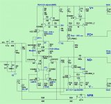
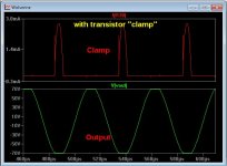
3. An example (below 2). Using the BJT (Q14) as clamp , some sort of saturation
induced oscillation on the negative clip.
Tried this on the real one - with TMC - a fast "chirp" of oscillation as the saturation
is clamped.
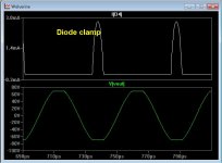
(Below 3 - diode) Just a fast diode between Q13 -C and Q12-B - no issue.
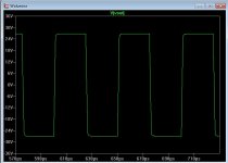
Notice I do get nearly symmetrical slew and clip ...
Short of overload , square wave response is not bad ( 4-close to symmetrical slew ).
So , there is a close example of the textbook amp .. . luckily ,both clamp options are
there.
Edit - this misbehavior must be addressed , the old japanese amps that DID
survive DID address this. Hey , this is not a "pinnae" amp , just a "working
man's" amp
 ..
..OS
Attachments
The base current only cancels at DC, if it cancels at all. It behaves almost exactly the same as it does in an LTP.
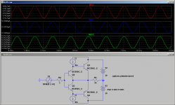
How you can explain this, simulated a LTP input (blameless) and complementary pnp/npn input (CFA)? The same source resistance, the same input filtar.
Attachments
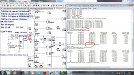
How you can explain this, simulated a LTP input (blameless) and complementary pnp/npn input (CFA)? The same source resistance, the same input filtar.
2nd confirmation - symmetrical TIS (below - diamond input).The LIN is not even close.
PS - same "everything" as the LIN , 1000% performance.
EDIT - NOT a true CFA (OPA 660 that runs on 80v rails
) RF amp !OS
Attachments
as just a bit unfair - try bootstrap cascoding the VFA diff pair
Something like this? I did not say that I not possible to make better LTP.
Attachments
Something like this? I did not say that I not possible to make better LTP.
That's cheating , try 50K.
(horrible offset)
edit - and it can't do 1KV/us , either ...(35mhz OP device BJT limit)
OS
Last edited:
Yes, the Diamond inputs were cascoded in your first example. If you cascode the LTP the performance becomes much better. Furthermore, your diamond has buffers as input transistors. Your LTP doesn't have any buffers.
In the Diamond input, the base currents and junction capacitances are both loads on the input. They both draw current with positive input, and sink current with a negative input. They add, rather than cancel.
In the Diamond input, the base currents and junction capacitances are both loads on the input. They both draw current with positive input, and sink current with a negative input. They add, rather than cancel.
Yes, the Diamond inputs were cascoded in your first example. If you cascode the LTP the performance becomes much better. Furthermore, your diamond has buffers as input transistors. Your LTP doesn't have any buffers.
In the Diamond input, the base currents and junction capacitances are both loads on the input. They both draw current with positive input, and sink current with a negative input. They add, rather than cancel.
But the current is low (uA).
(below- I input/ 140V p-p 4R load)
ahh , they DO add ... but only to 4 uA !
OS
Attachments
Last edited:
I didn't mean the performance would become better than the Diamond, I just meant the LTP becomes much more comparable to it when it's cascoded.
The idle currents cancel. The AC currents, which carry distortions, do not. Hence one way of reducing them is to cascode and/or buffer (exactly like Dadod's schematic). This applies for both LTP and Diamond.
The idle currents cancel. The AC currents, which carry distortions, do not. Hence one way of reducing them is to cascode and/or buffer (exactly like Dadod's schematic). This applies for both LTP and Diamond.
Last edited:
Yes, the Diamond inputs were cascoded in your first example. If you cascode the LTP the performance becomes much better. Furthermore, your diamond has buffers as input transistors. Your LTP doesn't have any buffers.
In the Diamond input, the base currents and junction capacitances are both loads on the input. They both draw current with positive input, and sink current with a negative input. They add, rather than cancel.
Those input transistors are not a buffer, thy are supper pairs, and could be connected as a diamond with similar result. EDIT: OK it could be called a kind of a buffer, but that buffer is not cascoded.
When you say "In the Diamond input, the base currents and junction capacitances are both loads on the input. They both draw current with positive input, and sink current with a negative input" and those currents flow the same resistor(input filter resistor and source resistor) isn't it subtraction and thus cancelation?
Last edited:
The input buffer is cascoded by the second pair of transistors which hold their Vce constant. Yes, it can be a Baxandall, cascode and buffer all in one. These names are all ideas, and they are not mutually exclusive.
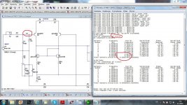
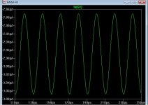
You can check for yourself in the simulator. See the attached plot. Yes, the base current of one transistor is positive and the base current of the other transistor is negative. But they respond in phase to the AC input signal. When the input voltage rises, both bases draw more current. While the idle currents cancel because they are opposite phase (+ and -) the AC currents do not because they are in phase.
You can check for yourself in the simulator. See the attached plot. Yes, the base current of one transistor is positive and the base current of the other transistor is negative. But they respond in phase to the AC input signal. When the input voltage rises, both bases draw more current. While the idle currents cancel because they are opposite phase (+ and -) the AC currents do not because they are in phase.
Attachments
Re stability of the cascode VAS: An old rule of thumb says that if you enclose more than 2 transistor stages in a feedback loop, the loop will need some sort of compensation. This has always been true in my experience. The cascode VAS has 3.
The problem with asymmetrical slew rates in the Lin topology is basically down to the CCS that loads the VAS being imperfect. Its output impedance falls at high frequencies. Self used positive feedback to counteract this. I found that with a 10mA CCS, and a VAS current limited to 20mA, the slew rates were reasonably symmetrical. However, replacing the CCS with another VAS is a nicer solution.
Ostripper, I split my last amp into driver and output stage boards in exactly the same way as you did. The only difference is that I included the protection on the driver board, so I have 2 more connections for the emitter resistor voltages. I also used the diode you mentioned to fix the clipping behaviour of the beta-enhanced VAS.
The problem with asymmetrical slew rates in the Lin topology is basically down to the CCS that loads the VAS being imperfect. Its output impedance falls at high frequencies. Self used positive feedback to counteract this. I found that with a 10mA CCS, and a VAS current limited to 20mA, the slew rates were reasonably symmetrical. However, replacing the CCS with another VAS is a nicer solution.
Ostripper, I split my last amp into driver and output stage boards in exactly the same way as you did.
The only difference is that I included the protection on the driver board, so I have 2 more connections for the emitter resistor voltages. I also used the diode you mentioned to fix the clipping behaviour of the beta-enhanced VAS.- Home
- Amplifiers
- Solid State
- Bob Cordell's Power amplifier book