When you clip, it's not going to sound good whether it's symmetrical or asymmetrical. Sounds like what you need is a lot of head room, a lot of swing in your case. Whether you use complementary or single end VAS with CCS tail is irrelevant. You can get a lot of swing with single ended VAS with CCS that pull heavier current. There is also an argument if you use complementary VAS, there are occasions that one side is going to turn off and you have crossover distortion also. with the CCS current tail, you don't turn off anything so you don't have crossover distortion.
I think I am good with 30W to 50W amp. I don't listen very loud. I know how loud 20W can be. I have a few guitar amps, it is very hard to crank it up pass 10W. I have power scaling on my amps, I cannot take 10W at full blast.
What is LIN?
Actually it's linn , but either google "classic Lin topology" or go to Bonsai's site ...
http://hifisonix.com/wordpress/wp-content/uploads/2014/01/CFA-vs-classic-Lin-VFA-topology.pdf .
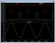
A complimentary VAS won't go class B on saturation .
I'll show (below) ....
-what a baxandall VAS does on clip.
Rounded like valves (tubes). Saturation is "clamped" (totally)
You say " it won't sound good" - but no worse than the 5% THD of
the loudspeaker. With this IPS , it's hard to tell when you are clipping -
short of a gross "hard clip".
Complimentary is also the same , just 2 LED CCS's. The only X-over
distortion is at the EF3.
BTW - with a level shifter , bob's IPS could run a symmetrical VAS ...
(luxman , many H/K amps).
OS
Attachments
I agree, the case for obsessive complementarity is overstated all too often.
One of the concerns I have as an amp designer is symmetrical slew rate and symmetrical drive of the OPS It seems with a Lin 'blameless' this is not easily achievable and Doug Self's proposals to rectify the situation are less than elegant (I am looking at his 3rd edition, pages 224 to 235 power amplifier design handbook). Typically, I take a worst case view that at certain frequencies, my speaker load may dip down to 3 Ohms or less.
OTOH, Bob uses a single ended JFET stage, but provides a symmetrical VAS stage through a diff amp + level shifter which although not entirely solving the symmetrical slew rate issue, at least provides symmetrical drive to the OPS. (I believe Hitachi also demonstrated something similar in the '80's in their now famous mosfet output stage amplifier application notes)
A few of us have gone for a balanced differential input to avoid the complication of the diff amp + level shifter that Bob uses.
I am not dismissing Bob's approach, but it seems to me that a complementary differential input is quite an elegant solution for a big power amp that provides direct drive to a complementary VAS with none of the slew rate issues you get on a Lin topology. For 20~70W amps, Lin topology seems ok for VFA designs - which is where most of Doug Self's professional designs seem to be focused for the high volume Hi-Fi market in his native UK.
The slew rate issues becomes ever more important IMV at higher powers if you stick to the 1~2V/us guideline.
For opamps and other small signal applications of course I am 100% behind the single ended diff amp approach - a balanced differential approach would be unnecessary. And, of course symmetrical just for the sake of it is nonsense.
")
(BTW OS - thanks for the plug! Appreciate it)
Last edited:
What's wrong with "obsessive complimentary".
They don't have to be complicated (below).
"What are the benefits" ?? OMG
10ppm - soft clipping - saturation is "tamed" - 150+v/us slew (even with a VFA).
- get this slew rate with 5ma VAS currents
I was a "LIN" fan up until a year ago - those days are gone.
Thermally, some of the complimentary's will cancel to the uA (VAS I).
PS- LIN is still good for "industrial" duty (subs /PA)
OS
I agree OS - this is why I use complementary topology designs.
Hi Edmond,
Since Cordell is not around here, could you comment this. http://www.diyaudio.com/forums/soli...lls-power-amplifier-book-481.html#post4170495
Later I've found that LTspice models for IRFP240/9240 have swapped Transconductance too.
Happy New Year
Damir
Since Cordell is not around here, could you comment this. http://www.diyaudio.com/forums/soli...lls-power-amplifier-book-481.html#post4170495
Later I've found that LTspice models for IRFP240/9240 have swapped Transconductance too.
Happy New Year
Damir
Hi Edmond,
Since Cordell is not around here, could you comment this. http://www.diyaudio.com/forums/soli...lls-power-amplifier-book-481.html#post4170495
Later I've found that LTspice models for IRFP240/9240 have swapped Transconductance too.
Happy New Year
Damir
Hi Damir,
Indeed, that looks strange. An error or typo? But you have to ask Bob himself.
Wishing you too a Happy New Year.
E.
Hi Bob,
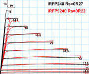
I am building a MOSFET amp with IRFP240/9240. I your book page 233, "Use of Source Resistors" you suggest to use dissimilar Source resistor to reduce crossover distortion, 0.15R for N-channel and 0.22R for P-channel mosfet.
Could you explain why you choose higher Source resistor for the P-channel mosfet, I would expect otherwise, lower Source resistor for the P-channel mosfet as it has lower Transcounductance. For example, Wishay IRFP240 min Transonductane is 6.9 S and for IRFP9240 it is 4.2 S.
One other thing I notice that your Spice models for those MOSFET have the Transconductance in reverse, IRFP240 Kp=4.8 and IRFP9240 Kp=9. Why so?
Best regards and Happy New Year
Damir
Hi Damir,
I'm sorry to be so slow in getting back to you. My wife has me looking for new carpeting, among a slew of other things. I have also been trying to finish my writeup of measurement results for resistor voltage-dependent distortion.
Its been awhile since I did those models, so I had to look up some old files to answer your question about the apparent reversal of Kp for the IRFP240 and IRFP9240 vertical MOSFETs. I believe those numbers are not reversed and are indeed correct. I realize it is non-intuitive for a P channel device to appear to have higher gm than an N channel device. However, I went back and even double-checked the IRF datasheets and it does appear that the IRFP9240 has greater gm than the IRFP240 at a given current. I re-simulated some of my device modeling SPICE test benches and it still seems to hang together.
Its been awhile, but I also seem to see that Kp by itself is not all there is to gm, and that the ratio of Kp of 2 devices in the model may not reflect the ratio of the gm of the 2 devices, both operating at the same drain current. Note that what is important is gm vs. Id.
Note also that tabular spec sheet numbers for minimum transconductance and not always all that useful, especially for evaluating SPICE models. I used actual IRF datasheet curves to make my models. I also did some lab measurements of individual devices.
I encourage others here to double check me on this. Errors are indeed possible and I always appreciate people pointing them out.
Cheers,
Bob
Question is simple...considering that i will be using the same output, is C1 value correct?
I need a simple answer...yes or no..then i will search for my own mistakes in the pcboard parasitic capacitances and inductances.
My circuit is modified..but current to VAS is the same and output i built the same to check this capacitance value.... i will modify my way...but i need to know if this value is correct or if was a revision mistake...maybe 130pf is the value, as i found it as the smallest stable value to use in my particular circuit.
Values in the VAS are different..but i made it the same as your schematic to check because my way was not working...but your way also not worked....i have built the VAS, and the output the same as your schematic in order to check the value..also the VAS current is the same you use..also the supply voltage is the same you use....made this way to check....then i will make it my way as the input is different in my circuit and also the output.
Thank you in advance by the time spent.
regards,
Carlos
Hi Carlos,
The 30pF in Figure 3.12 is the correct value. It creates a closed loop bandwidth of about 525kHz, which is the target for most of the illustrative designs in Chapter 3. I went back and resimulated that design and there seems nothing unusual. I at first was worried that there was stability trouble in the cascode VAS, but did not see any. Note the transistors used in the output stage. The finals are MJL21193/4, a bit slow by today's standards, but used in the examples to illustrate typical performance that can be had when using output transistors of mid-range speed. Are you using faster/different transistors? Same question for the transistors being used in the Darlington-cascode VAS.
Cheers,
Bob
Increasing the current of the CCS in the VAS stage will speed up the slew rate. You just need enough current to charge and discharge the capacitance.
I can't find the book reference, but basically using ( I X t= V X C) where t is the time used for slew rate. So I=VC/t.
Yes, this is from the fundamental "law" of a capacitor, i = C x dv/dt. Rearranging gives the signal slope = dv/dt = i/C
If the maximum current available to charge the capacitance is I we then have slew rate = dv/dt (max) = I/C
Very good one.... have beated mine Dx Mark One.
Well....it can go lower if i figure out how to use 33pf as compensation
Your amplifier goes much lower than 0.0048% loaded with 8 ohms.... but have to tweak and get out from the exactly calculated values..some drift from the optimize values reduces THD.... some out of the box thinking.
Your Cascode VAS is a great contribution to our community.... great one.... i may use your circuit if i figure out (or if you help me) how to use 33pf as compensation.
regards,
Carlos
Hi Carlos,
Were these measured or simulated results?
BTW, I first used the Darlington-cascode VAS in my MOSFET power amplifier with error correction. It was especially helpful with the VAS transistors I used back then, which were not as good as those available today.
Cheers,
Bob
I'm sorry to be so slow in getting back to you. My wife has me looking for new carpeting, among a slew of other things.
So your slew rate has been exceeded? (OK. Really lame nerd humor...)
Hi Mr. Cordell.
I have a question after seeing Carlos using your schematic in Fig. 3.12 in page 68 in your book.
I am hesitant in building a SS power amp for the reason that you described the complementary differential stage is superior because it's lower distortion. I always have a believe that for good sound, less is more. I really don't want to build the complementary differential input. Not only you have to double the LTP stage, you have to put in over current protection to avoid the VAS from drawing excess current. The more circuit, more more chance to cross couple and susceptible to EM interference.
Thanks and Happy New Year.
Alan
My question to you is: Is it true that the only disadvantage of the non complementary differential input stage is more even harmonics? Which is mainly 2nd harmonics? If that is the case, it's not the end of the world. From my understanding, it's the odd harmonics ( particular 3rd) that is offensive and unpleasant to the ears. Even harmonics are ok. particularly 2nd gives the warmth.
Hi Alan,
I do not necessarily prefer the full complementary input stage (PNP LTP + NPN LTP) over what I refer to as the unipolar IPS (one LTP, either NPN or PNP).
What really matters is having a push-pull VAS rather than a single-ended VAS loaded with a current source. The full complementary IPS is just one convenient way to drive a push-pull VAS - and it looks nice and symmetrical on the schematic
.I also do not subscribe to the generalization that fewer transistors leads to better performance or sound.
In most of my designs I use a unipolar IPS driving a push-pull VAS. There are several ways to do this described in my book. One good early example of this was Tom Holman's APT 1 amplifier.
I generally prefer JFET inputs, and that often dictates using an N-channel unipolar IPS, since P-channel duals are not readily available. I have always been able to get just as good, if not better, performance from a unipolar IPS driving a push-pull VAS. This was the approach I used in my MOSFET power amplifier with error correction of long ago in the early Eighties.
Cheers,
Bob
So what is the benefit of a complimentary input stage apart from the input bias current cancellation. Is it the symmetry of the transient pulse obtained ?
Regards
Arthur
Hi Arthur,
As I alluded to above, the benefit of the full complementary input stage is mainly that it is a convenient way to drive a push-pull VAS. In my opinion, the push-pull VAS is the end goal, and there are several ways of driving it with unipolar LTP input stages. Some examples can be found in Section 7.4 in my book.
Input bias current cancellation is not much of an issue, since betas of the NPN and PNP pairs are not likely to be the same unless you get lucky. If they differed by a factor of 2, you would only get half cancellation. Also, note that several designers use a full complementary IPS implemented with JFETs, where input bias current cancellation is not an issue.
Cheers
Increasing the current of the CCS in the VAS stage will speed up the slew rate. You just need enough current to charge and discharge the capacitance. No magic about this.
As shown in Fig. 7.1 in p128. if you increase I2 from 10mA to say 25mA, you'll increase the slew rate so that becomes a non issue. I can't find the book reference, but basically using ( I X t= V X C) where t is the time used for slew rate. So I=VC/t. if you know the C, you can plug in how many volts per uS into V and t. Then you can calculate the current I to give you the slew rate.
It doesn't matter if one side is faster as long as the slow side exceeds the minimum requirement of the slew rate.
Hi Alan,
Two things to keep in mind. First, the push-pull VAS gives twice the peak drive current to the output stage for a given idle current. So it has a dissipation advantage for the VAS transistor and is better at driving a 2 EF output stage, where output stage current gain is marginal, especially when there is beta droop in the output stage transistors at high current drive levels.
Also, symmetry in the VAS is desirable, and equal slew rate capability in both directions is a worthy goal (although slew rate is not always dictated by VAS current capability).
Cheers,
Bob
What's wrong with "obsessive complimentary".
They don't have to be complicated (below).
"What are the benefits" ?? OMG
10ppm - soft clipping - saturation is "tamed" - 150+v/us slew (even with a VFA).
- get this slew rate with 5ma VAS currents
I was a "LIN" fan up until a year ago - those days are gone.
Thermally, some of the complimentary's will cancel to the uA (VAS I).
PS- LIN is still good for "industrial" duty (subs /PA)
OS
Hi OS,
This is a nice design, indeed. However, in my opinion, its very good performance has more to do with a well-engineered push-pull VAS than the use of a full-complementary IPS.
Cheers,
Bob
I wholeheartedly wish Carlos luck to use Bob's LIN example.
It works (below) ... I use it as my "tester" , as it is SO "rock solid"
at ANY rail voltage.
Spilled the wine on it - it still worked
PS - still , myself and most others prefer the "faster" complimentary
IPS's - they are more "engaging" (I no longer believe all amps sound the same).
OS
Thanks OS; nice implementation.
BTW, the many examples of the LIN architecture in my chapter 3 was mainly to explain the basic principles and tradeoffs in amplifier design. It is not intended to imply that I think the LIN topology is the preferred amplifier design. It certainly has been a reliable workhorse over the years, however. And it can yield very good performance when its design is optimized.
Cheers,
Bob
Hi Damir,
I'm sorry to be so slow in getting back to you. My wife has me looking for new carpeting, among a slew of other things. I have also been trying to finish my writeup of measurement results for resistor voltage-dependent distortion.
Its been awhile since I did those models, so I had to look up some old files to answer your question about the apparent reversal of Kp for the IRFP240 and IRFP9240 vertical MOSFETs. I believe those numbers are not reversed and are indeed correct. I realize it is non-intuitive for a P channel device to appear to have higher gm than an N channel device. However, I went back and even double-checked the IRF datasheets and it does appear that the IRFP9240 has greater gm than the IRFP240 at a given current. I re-simulated some of my device modeling SPICE test benches and it still seems to hang together.
Its been awhile, but I also seem to see that Kp by itself is not all there is to gm, and that the ratio of Kp of 2 devices in the model may not reflect the ratio of the gm of the 2 devices, both operating at the same drain current. Note that what is important is gm vs. Id.
Note also that tabular spec sheet numbers for minimum transconductance and not always all that useful, especially for evaluating SPICE models. I used actual IRF datasheet curves to make my models. I also did some lab measurements of individual devices.
I encourage others here to double check me on this. Errors are indeed possible and I always appreciate people pointing them out.
Cheers,
Bob
Hi Bob,
Thank you very much to be patient with me. What I am trying to decide where to use higher value Source resistor in N-channel or in P-channel mosfet to get better complementary behavior.
I have mosfets fro Vishay and the data sheet says:
for IRFP240 min forward Transonductance gfs is 6.9 S at VDS = 50 V, ID = 12 A
for IRFP9240 min forward Transconductance gfs is 4.2 S at VDS = - 50 V, ID = - 7.2 A
I am not sure how parameter Kp represents that.
Here is one example of the measurement taken with a tracer for the same mosfet types but produced by IR.
Best wishes in New Year
Damir
Attachments
One of the concerns I have as an amp designer is symmetrical slew rate and symmetrical drive of the OPS It seems with a Lin 'blameless' this is not easily achievable and Doug Self's proposals to rectify the situation are less than elegant (I am looking at his 3rd edition, pages 224 to 235 power amplifier design handbook). Typically, I take a worst case view that at certain frequencies, my speaker load may dip down to 3 Ohms or less.
OTOH, Bob uses a single ended JFET stage, but provides a symmetrical VAS stage through a diff amp + level shifter which although not entirely solving the symmetrical slew rate issue, at least provides symmetrical drive to the OPS. (I believe Hitachi also demonstrated something similar in the '80's in their now famous mosfet output stage amplifier application notes)
A few of us have gone for a balanced differential input to avoid the complication of the diff amp + level shifter that Bob uses.
I am not dismissing Bob's approach, but it seems to me that a complementary differential input is quite an elegant solution for a big power amp that provides direct drive to a complementary VAS with none of the slew rate issues you get on a Lin topology. For 20~70W amps, Lin topology seems ok for VFA designs - which is where most of Doug Self's professional designs seem to be focused for the high volume Hi-Fi market in his native UK.
The slew rate issues becomes ever more important IMV at higher powers if you stick to the 1~2V/us guideline.
For opamps and other small signal applications of course I am 100% behind the single ended diff amp approach - a balanced differential approach would be unnecessary. And, of course symmetrical just for the sake of it is nonsense.
(BTW OS - thanks for the plug! Appreciate it)
Hi Bonsai,
I agree with everything you have said here. My only caveat is unipolar vs full complementary IPS. They both can be made very good, and they both have their own shortcomings or technical challenges. Pick your poison.
One of the biggest shortcomings of the full complementary IPS is that it generally forces you to go to a BJT IPS. I strongly prefer a JFET IPS. Among other things, if you believe that EMI at the input can degrade sound quality, then note that a JFET input is much more tolerant of EMI, since you are not looking into forward-biased base-emitter junctions, which are happy to rectify, as opposed to a reverse-biased gate-channel junction.
Cheers,
Bob
Resistor voltage-dependent distortion results
Here I’ll describe and discuss the results of my resistor voltage dependence distortion tests that I discussed in my earlier post.
We note for reference that a resistor with Kv = 1 ppm/V with 10V rms across it will produce 10/5.9 = 1.7 ppm H3 = -115 dB = 0.0017% H3. This is what is given by Bruce Hofer’s equation: H3 = Kv * Vs / 5.9.
Measured H3 for the 6.8k 1/4 W carbon composition resistor ranged from –127dB (0.45ppm) to –102dB (8ppm) for applied rms voltage from 2.5V to 10V. H3 thus increased by 16 times over this 4:1 voltage range, suggesting that H3 goes as Vs squared. This is at variance with Bruce’s equation.
Put another way, inferred Kv for the resistor ranged from 1.05 ppm/V to 4.7 ppm/V over this 4:1 voltage range. This suggests that Kv is not constant, but rather proportional to voltage. This is further made plausible by the fact that a crummy carbon composition resistor exhibits a Kv of less than 5 ppm/V at 10V rms.
If we calculate the number for voltage dependence in ppm/Vsquared, it varies from 0.071 to 0.091 over this voltage range, suggesting that this is the number that may be a constant that describes the voltage-dependence of the resistor. The variance of this measured number here can be explained by a dB or so of measurement error here and there. The measured variances were somewhat random over the range, and certainly not monotonic.
Absence of thermal distortion at the test frequency of 1kHz was confirmed by tests at 10V rms at 500Hz and 2kHz that showed the same level of H3.
A 6.8k ¼ W carbon film resistor was next measured. Its H3 ranged from -131dB (0.28ppm) to -119dB (1.1ppm) for applied voltage ranging from 6V rms to 10V rms. H3 for voltages less than 6V were too small to be reliably measured by this setup. For this 1.7:1 range of Vs, H3 changed by a factor of 3.9. Once again, this suggests that H3 is rising at a rate closer to the square of Vs. Over this same voltage range, inferred Kv ranges from 0.28 ppm/V to 0.66 ppm/V.
A 6.81k 1/4W metal film resistor was next measured. Its H3 was very low and not reliably distinguishable from test setup residual. I was not able to draw any conclusions from it other than that it must have had Kv much less than that of the carbon film resistor, as expected. Assuming that its H3 was -135dB at 10V rms, and using Bruce’s formula, Kv might be estimated to be 0.1 ppm/V. This is within reason, but at the very good end of expected performance for an ordinary metal film resistor.
How to check Bruce’s equation?
A SPICE distortion simulation was run in order to check to see if H3 was proportional to Vs or to Vs squared with a simulated voltage-dependent resistor. A resistor with known Kv was created with a JFET voltage controlled resistor arrangement with gate feedback, much like the JFET agc element used in an oscillator. With approximately 50% gate feedback, second harmonic of the resistance as a function of signal is eliminated, leaving a resistance characteristic with voltage dependence wherein resistance increases slightly with applied voltage of either polarity. This emulates a real-world resistor with voltage dependence (with the exception of the sign of Kv, which should not matter).
DC bias was applied to the gate of the JFET to establish its nominal resistance and the JFET was configured as the shunt element in a 40dB attenuator. Kv of the JFET was measured to be 16,000 ppm/V by dc simulation, and was verified to be constant within the range of voltages used in the simulation. Signal voltage was applied across the JFET resistor ranging from 2.5mV peak to 20mV peak at 1kHz. H3 ranged from 3.3ppm to 27ppm, respectively. H3 was proportional to signal amplitude, as predicted by Bruce’s formula H3 = Vs * Kv / 5.9. This simulation largely confirmed the correctness of Bruce’s equation for resistances with a constant value of Kv independent of voltage.
Assuming my real-world measurements are reasonably accurate in showing a voltage-squared H3 amplitude dependence, I’m inclined to conclude that Kv of a real-world resistor is voltage-dependent. Such a behavior of Kv would explain and resolve any differences between my findings and Bruce’s equation.
None of this is to say that resistor voltage distortion is not important or that resistors are better than some have suggested. Indeed, if Kv goes as Vs squared, it is easy to see how some of these resistors would create distortion in a power amplifier with several tens of volts across the feedback resistor.
There is another caveat. Although my results seem to suggest that Kv may be a function of voltages for the carbon-based resistors I measured, this does not necessarily hold for resistors made from other resistance materials.
What do you all think about the hypothesis that Kv for a real-world resistor is voltage dependent?
Cheers,
Bob
- Home
- Amplifiers
- Solid State
- Bob Cordell's Power amplifier book