I have mentioned it more than a few times.PCB layout and grounding
................. note that a loudspeaker load will lead to non-linear currents even with a linear output voltage so the most important thing is to minimise efficiency of radiation (out and return paths twisted together) (I do not believe that I have ever seen anyone make this observation before - this is a potential source of distortion in audio power amplifiers when driving real-world loads rather than the usual test-bench resistor. Further investigation is required. Has anyone any references for this?)..................
At least one post describes taking the speaker return to the amp PCB and then following the route of the high current path to the PSU input and then follow the PSU cable to the main audio ground. The loop area of the WHOLE route should be minimised.
Dr Cherry also talks about this and in one article shows a PCB layout that tries to minimise the spkr return loop area. But in it he makes what I would call a mistake and forgets about the final part of the route from PCB to where the PSU cabling passes over the Main Audio Ground.
He then bootstrapped the cascode from the LTP tail with AC coupling, placing the cascode DC bias at about half the positive rail voltage.
Hi Bob,
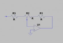
I am a bit puzzled by this arrangement (ed. 5, page 96, figure 4.16.b)
because the output of the CCS of the tail pair which is expected to be at highy impedance sees a 100 kOhm load connected to the AC ground (via C3 and the positive power supply).
Has this 100 kOhm resistor not a deleterious effect ?
Some schemes provide another CCS to supply the polarising network here R5//C3. Are they not better ?
To further enhance stability margins in the ANF current source, a 2k2 resistor in series with the base of the control transistor is shunted by a 10pF~22pF capacitor as shown below.
The capacitor introduces a zero close to the unity loop gain frequency; this increases phase margin from 83 degrees (blue trace) to 114 degrees (green trace).
Neat idea, Mike. 114 degrees is a relative plethora of phase margin
") .
.Cheers,
Bob
All my jFets have max Vds from 25V to 50V.
The k389 & k246 are both 50Vds
Borbely uses the k246 extensively in his designs.
Pass frequently comments that the k170 can be run at it's maximum Vds and even above.
I wonder if the k246 can similarly be run @, or just above, 50Vds?
Could any of the small Zetex mosFETs be used as cascodes for the input stage?
Hi Andrew,
The new LSK489 Dual monolithic JFET from Linear Systems is rated at 60V.
Cheers,
Bob
Bob, one of the best bits in your book is the chapter on measurements including the list of test equipment that might be usefully obtained on eBay.
It shows the measurement of various distortions using soundcards is now possible for impecunious beach bums who are versed in the art. (Certainly, emerging from the bush this Millenium, I can now measure speakers & mikes ... more accurately in my shed than I could in Jurassic times with anechoic chambers and (then) SOTA gear.)
But one thing that has come out of this thread is the usefulness of measuring the Closed Loop response of amps to Zillion MHz.
In your 2nd edition, could you perhaps expound a little on how to do that simply and cheaply.
Hi kgrlee,
Thanks for the kind words about the measurement chapter. I do hope to take that chapter further, especially given that more good PC - based stuff has come out since my book. In fact, some of the stuff members have done here on several threads is really inspiring.
As far as HF goes, I go to 10MHz in my lab with a combination of an HP 652A audio generator (a great old tank) and an HP 400EL or HP3400 AC voltmeter, both of which go to 10MHz (all obtained on Ebay). To go higher I have the Tek (SG502?) TM500 RF oscillator that goes up to in the low hundreds of MHz. I don't presently have an AC voltmeter that goes up above 10MHz, so I use a scope. My Tek analog scope only goes to about 100MHz, but I have an Agilent DSO that samples at up to 8 Gs/s and has analog bandwidth up to 1.5 GHz.
As far as what can be done cheaply up to those frequencies, maybe I can come up with some DIY purpose-built designs that can go up to 10MHz for sinewaves generated with R-C circuitry and maybe something else to go up much higher with tunable RF circuitry. With today's IC's, it should not be difficult to do an AC voltmeter that goes up to 100MHz. But for all I know, one may be able to get this stuff on Ebay anyway
.Bottom line: This is worth some discussion in that chapter of the new edition.
Thanks for the suggestion.
Cheers,
Bob
So you're at page 442 of the book trying to determine some SPICE parameters for vertical MOSFETs -- here's a video I put together on using Microsoft Excel's "Solver" add-in to calculate values of Vth, KP and Lambda:
MOSFET Solver - YouTube
MOSFET Solver - YouTube
I have mentioned it more than a few times.
At least one post describes taking the speaker return to the amp PCB and then following the route of the high current path to the PSU input and then follow the PSU cable to the main audio ground. The loop area of the WHOLE route should be minimised.
Dr Cherry also talks about this and in one article shows a PCB layout that tries to minimise the spkr return loop area. But in it he makes what I would call a mistake and forgets about the final part of the route from PCB to where the PSU cabling passes over the Main Audio Ground.
Hi Andrew,
The potential for magnetic radiation caused by supply currents in class-B amplifiers to give rise to distortion is indeed well-known, however there is a potential extra "gotcha" with real-world loads that I have not seen discussed before. I am aware of the Cherry reference; it is entitled "A New Distortion Mechanism in Class B Amplifiers" and I agree that his proposed solution is flawed. Douglas Self and Bob in their books also talk about distortion caused by radiation induced by the supply currents in class-B amplifiers. However, in all of these cases, the amplifier load is assumed to be linear - i.e. if you apply a sinusoidal voltage with 0% harmonic distortion, a sinusoidal current with 0% harmonic distortion will be drawn.
In such a situation, if the wiring of the power supply is arranged such that radiation of the positive and negative half cycles couple equally to sensitive parts of the amplifier, the radiation is effectively "linear" and will not cause distortion.
However, and this is the part that I have never seen discussed anywhere before: real loudspeakers are non-linear loads that draw distorted current waveforms even when driven by voltage waveforms with 0% harmonic distortion. In this case, even if the power supply wiring is arranged such that radiation of the positive and negative half cycles couple equally to sensitive parts of the amplifier, the radiation will no longer be effectively linear (because the load is drawing a non-linear current) and distortion could be induced. It therefore becomes important to minimise radiation from the supply wiring, not merely ensure that radiation from the positive and negative rails is symmetrical.
Last edited:
Hi Bob,
Could we have an update on the status of a second edition of your book? Has the publisher given the go ahead? When are we likely to see it?
Hi Harry,
The second edition is about a year out. I do have some flexibility in the date, and some dependence on the amount of time my dear wife Angela will let me spend on it. I'm guessing it will come in at between 700 and 750 pages. There is certainly no lack of good material.
I am deeply indebted to you and the other the members of this forum for inspiration that led to the first edition, and that will certainly be the case for the second edition. This thread has helped me greatly in formulating and prioritizing material for the second edition. It is an honor to get so much input from so many smart, dedicated and creative people who participate here.
Cheers,
Bob
It would appear A&R Cambridge were concerned about instability in the amplified negative feedback (ANF) current source in their A60 amplifier.
They used a 1nF capacitor shunting the collector of the control transistor of all their ANF current sources instead of using a resistor in series with the base of the control transistor:
http://www.retrohifi.co.uk/a60_amp_service_manual.pdf
I simulated the ANF current source loop gain with the 1nF shunt capacitor across the collector of the control BJT and it does indeed reduce loop gain at high frequencies by introducing a dominant pole at about 20KHz.
The blue trace gives the loop gain with the shunt capacitor, while the green trace gives the loop gain without the capacitor.
Hi Mike,
Thanks for bringing this to our attention and analyzing their circuit. Looks like they moved the ULGF from about 60MHz down to about 20MHz, if I interpret your plot correctly. This certainly makes sense.
Cheers,
Bob
Harry, I remember this being discussed by several members who exiled themselves long ago (Andy_C, GK, MJL21193 and so on). As I understand the rails need to be coupled together WITH the load return so that the load field is canceled as well. This need to be done without polluting any ground references. It would seem to be the task for a ground plane.
However, the output L/R probably radiates most, so as I have proposed in other places, why not locate the L remotely (behind the heatsink?) with a twisted pair leaving the R at the PCB?
However, the output L/R probably radiates most, so as I have proposed in other places, why not locate the L remotely (behind the heatsink?) with a twisted pair leaving the R at the PCB?
Bob,
For a long time I have been promising some feedback on your book. I will PM you a list of typos but there's other feedback which I imagine may stimulate further discussion/be of interest to everyone so I shall post it here:
page 19, the section on Early Effect states that if the curves in fig. 2.1 are extrapolated back to the x-axis, they will all intersect at the Early Voltage. Strictly speaking this would only be true for all transistors if the parameter for figure 2.1 was Vbe rather than Ib (see for example Analysis and Design of Analog Integrated Circuits 5th Edition International Student Version by Gray, Hurst, Lewis and Meyer, page 15).
page 72 - no mention of how adding further output devices will degrade phase margin (although this is mentioned later on page 212). Also, the 2SC3503/2SA1381 pair has been discontinued by Sanyo; fortunately Fairchild continue to manufacture the identically specified KSC3503/KSA1381.
page 201 - you should mention that in order to minimise inductance, outward and return current paths must enclose as small an area as possible - "non inductive" resistors standing up perpendicular to the board can actually have a higher than expected effective parasitic inductance.
Thermal stability of output stage bias setting
In several places in the book, you mention mounting of Vbe multiplier transistor onto output heatsink, but mounting directly to backside of output transistor is better, as both you yourself note in the book and Douglas Self mentions in his book.
Matched-pair devices for input stage
Are you familiar with the SSM2212 and SSM2220 matched low-noise NPN/PNP pairs from Analog Devices? I've never used them but the specifications look good and they probably deserve a mention in your book (Vce is low and Ccb is high so cascoding is highly recommended)
Output devices in your BJT-output amplifier examples
In the majority of the BJT-output amplifiers in your book, you use very slow transistors in the output stage, both for the drivers and the final output devices. This in turn imposes severe limitations on ULGF and therefore audio-band loop gain. Additionally, these slow devices tend to have other poor attributes such as high levels of "beta-droop". I can't help thinking that perhaps you've done this to make MOSFET-output amplifiers look better? Given the low cost and high performance of ON's MJL1302/3281 etc. pairs, I don't know why you don't just use those in all your BJT-output amplifier examples. Also, try the Fairchild KSA1220A/KSC2690A pair as drivers (Toshiba 2SA1930/2SC5171 are better but are to be discontinued).
PSRR
Please could you add more about PSRR, especially how different compensation techniques will result in different PSRR.
PCB layout and grounding
In the sections on PCB layout and grounding, I feel that these would benefit from significantly more diagrams - pictures here are much easier to understand than written description, with less possibility for misinterpretation. For distribution of the amplifier's power rails, you should explain that if you twist/interleave +/-, this doesn't "cancel" the magnetic field. Rather, magnetic field is still generated, but now it's "linear" (much reduced harmonic content). Also, note that a loudspeaker load will lead to non-linear currents even with a linear output voltage so the most important thing is to minimise efficiency of radiation (out and return paths twisted together) (I do not believe that I have ever seen anyone make this observation before - this is a potential source of distortion in audio power amplifiers when driving real-world loads rather than the usual test-bench resistor. Further investigation is required. Has anyone any references for this?).
Loop-gain simulation
I'd like to add to the previous requests that you cover loop-gain simulation in more depth, including how to set up proper Middlebrook Probe simulations.
Graphs
This is a subjective thing but personally I'd like to see gridlines on all your graphs.
Counterfeit devices
I think it would be worth mentioning the existence of counterfeit devices and the problems they create. Also provide advice on how to avoid buying them and how you could verify if devices you have bought are genuine.
solid-state relays
Please add discussion of solid-state-relays to the section on relays. Modern 150 V rated MOSFETs have low-enough Rdson that distortion is probably lower than standard relays, not to mention all the other benefits of solid-state. Bonsai has a good article on solid-state relays on his hifisonix website.
Balanced input stages
Please could you add a lot more discussion of balanced input stages, including quantification of distortion performance and more options that don't use JFETs (hard to source).
Class-D
Are you familiar with Bruno Putzey's "A universal grammar of class D amplification"? This is a useful reference. A PDF is available from Hypex's website, and an audio recording of a presentation to the AES is available in the AES member section.
Switching loss not accurately described. You refer to the losses incurred in driving the gate of the device as "switching loss", but the term "switching loss" is more normally reserved for the losses incurred as the power device traverses the linear region when switching from the "on" state to the "off" state or visa-versa. During these periods, Id and Vds can be simultaneously large, resulting in instantaneous device power dissipation of several hundred W. Fortunately the switching transients only last a few 10s of nano-seconds.
Driving the gate is usually a lossy process because the traditional technique used is to drive the gate with a voltage source (gate driver) via a resistor. As the gate's capacitance is repeatedly energised/de-energised, power is dissipated in the gate driver's output resistance, the gate resistor and the MOSFET's internal gate resistance. However, the gate capacitor is a fairly high-quality (low-loss) capacitance and there is no inherent need for the energising/de-energising of this capacitance to be a lossy process. If resonant techniques are used, the energising, de-energising, or both, stages of driving the gate can be made a closer-to-lossless process. Please see A First Approach to a Design Method for Resonant Gate Driver Architectures.
Hi Harry,
Wow! What a wonderful list of suggestions. I agree with every one of them.
Thank you so very much for compiling this.
One thing that has been prominent on my priority list has been to improve/expand the five chapters on Class D. This is a fast-moving area and is also an area where I am still learning a lot. Bruno in particular is a brilliant inspiration in this area. Thanks for bringing that resonant gate driver technique to my attention.
Thanks again!
Cheers,
Bob
To further enhance stability margins in the ANF current source, a 2k2 resistor in series with the base of the control transistor is shunted by a 10pF~22pF capacitor as shown below.
The capacitor introduces a zero close to the unity loop gain frequency; this increases phase margin from 83 degrees (blue trace) to 114 degrees (green trace).
This method preserves gain the best, and uses the smallest components AFAIK. I'm curious, are the results the same when you substitute the sense transistor with a transistor with much lower Cje? If so then, for most small-signal transistors an extra B-E cap is in order.
However, does any of this affect the output impedance of the CCS significantly? After all, the feedback point is not at the output and so the impedance of this CCS is entirely at the mercy of the Early effect and Cbc of the output transistor. Is it worth using more than a single component to stabilize it?
Harry, can you send me a copy of the above paper? Thanks.
Hi Harry,
Me too, if possible.
Cheers,
Bob
Hi Bob,
I am a bit puzzled by this arrangement (ed. 5, page 96, figure 4.16.b)
because the output of the CCS of the tail pair which is expected to be at highy impedance sees a 100 kOhm load connected to the AC ground (via C3 and the positive power supply).
Has this 100 kOhm resistor not a deleterious effect ?
Some schemes provide another CCS to supply the polarising network here R5//C3. Are they not better ?
Hi forr,
I agree that the 100k impedance shunting the LTP tail can be potentially deleterious. I have in the past recommended using a PNP emitter follower to tap the tail voltage and buffer it. A Zener or the like in the emitter circuit then provides the voltage offset to bias the cascode bases at the nominal DC level desired. A P-channel JFET would also suffice. In fairness, and being a bit picky, either of these approaches adds a junction capacitance to the potentially sensitive tail node, while the 100k resistor essentially does not (I'm thinking of EMI here). One might argue that this suggests using a P-channel JFET in preference to the BJT PNP if one is going to use an active device to buffer the tail voltage (no forward-biased junctions).
Cheers,
Bob
Just barely on the same subject, I found a useful page here:
Resistor's behavior at HF and VHF.
So a 100k resistor at the emitter probably contributes .33pF or so. I contacted the author and he said if the resistor were lowered from 3/8" to 1/4" to the ground plane, capacitance to ground would increase by .33pF. So, capacitance of that resistor should not be more then 2pF I think, even if you use a ground plane.
On the topic of passive components, maybe you can discuss this in your book?
Bruno Putzeys r4 random rants, raves and ramblings
It is interesting that a linear pot would give very low distortion. Based on this, Rod Elliot's mod to make log pots out of linear ones could be one of the best volume control options. However I'd really like to see what Bruno envisions when he mentioned putting it in the feedback loop. Shunt, series, or feedback from the wiper? Any of these options could be done safely with bypass resistors, unless the point is to present the wiper with the full opamp input impedance and minimize current.
Last edited:
On the topic of passive components, maybe you can discuss this in your book?
Bruno Putzeys r4 random rants, raves and ramblings
It is interesting that a linear pot would give very low distortion. Based on this, Rod Elliot's mod to make log pots out of linear ones could be one of the best volume control options. However I'd really like to see what Bruno envisions when he mentioned putting it in the feedback loop. Shunt, series, or feedback from the wiper? Any of these options could be done safely with bypass resistors, unless the point is to present the wiper with the full opamp input impedance and minimize current.
I'm not sure if this is what Bruno had in mind.
I used this many years ago to get a log response from a linear pot.
Attachments
- Home
- Amplifiers
- Solid State
- Bob Cordell's Power amplifier book