Hi Bob,
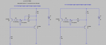
Thank you Bob, and here is next simulation were the cascode base driving signal connected to a replica of the feedback signal, with a bit worst result then if driving from the tail. Could be because the phase difference?
BR Damir
Hi dadod,
Thanks for doing this!
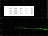
If I read correctly, the replica THD20 was 0.00012% while the tail-driven THD20 was 0.00008%. So the replica version distortion is 50% higher, but still a very very small number compared to the 0.025% number without driving the cascode.
Excellent!
Cheers,
Bob
Cascoded LTP IPS
I like the very simple IPS cascode in #4 of tpc-vs-tmc-vs-pure-cherry which is via Guru Wurcer.
It's good for 50W amps and may ju..ust do 200W @ 4R. If anyone has ideas for suitable small signal FETs in this position for big amps, please post. FET i/ps seem to benefit most but BJT i/ps have the edge of THD in my simple amp.
The models I used were Scott Wurcer's from discrete-opamp-open-design
I found (in SPICE world) they only made a diff when THD20k dropped below 10ppm so your other stuff needs to be good too. In the #4 circuit, it brings THD20k down to 1ppm from 2ppm.
I have not tried this for real. My Jurassic 'real life' experience with (BJT) cascode IPSs was they introduced overload problems and any advantage was invisible cos I couldn't measure THD20k reliably to better than about 30ppm in dem days.
Scott says the 'real' practical advantage isn't 1ppm THD20k ... but that THD doesn't get worse when the impedances at the 2 i/ps of the LTP are mismatched. eg if the amp is fed by a 10k pot.
I went through a phase when I religiously matched input & feedback impedances on loadsa circuits cos this ... but I've grown out of it.") Didn't know a 'cure' in dem Jurassic days.
Didn't know a 'cure' in dem Jurassic days.
I like the very simple IPS cascode in #4 of tpc-vs-tmc-vs-pure-cherry which is via Guru Wurcer.
It's good for 50W amps and may ju..ust do 200W @ 4R. If anyone has ideas for suitable small signal FETs in this position for big amps, please post. FET i/ps seem to benefit most but BJT i/ps have the edge of THD in my simple amp.
The models I used were Scott Wurcer's from discrete-opamp-open-design
I found (in SPICE world) they only made a diff when THD20k dropped below 10ppm so your other stuff needs to be good too. In the #4 circuit, it brings THD20k down to 1ppm from 2ppm.
I have not tried this for real. My Jurassic 'real life' experience with (BJT) cascode IPSs was they introduced overload problems and any advantage was invisible cos I couldn't measure THD20k reliably to better than about 30ppm in dem days.
Scott says the 'real' practical advantage isn't 1ppm THD20k ... but that THD doesn't get worse when the impedances at the 2 i/ps of the LTP are mismatched. eg if the amp is fed by a 10k pot.
I went through a phase when I religiously matched input & feedback impedances on loadsa circuits cos this ... but I've grown out of it.
Didn't know a 'cure' in dem Jurassic days.
Last edited:
It sounds like your amplifier has a high frequency stability problem.
Although Monte Carlo can be useful in finding weaknesses in a design for certain combinations of component variations, it is important that the design be robust by design before doing a Monte Carlo.
Bob
Hi Bob,
My simple observation: when an amplifier topology built from complementary inputs with current mirrors is used, it is much more critical to match transistors then when resistor loads are used. High gain from current mirrors demands close transistor matching.
For my simulations where BC550C are used for the input differential pair with current mirrors loads, if a BC550A is substituted for ONE of the diff-pair transistors a Monte Carlo analysis will not complete.
For my simulations where BC550C are used for the input differential pair with resistor loads, if a BC550A is substituted for ONE of the diff-pair transistors a Monte Carlo analysis will complete with a modest increase in THD.
BC550C hfe=420-800
BC550A hfe=110-220
A 600W @4ohm proto with BC550C and BC560C sounds swell. I'm just not sure an international company relying upon local repair shops would select the complementary current mirror load topology.
Attachments
Can you explainFor my simulations where BC550C are used for the input differential pair with current mirrors loads, if a BC550A is substituted for ONE of the diff-pair transistors a Monte Carlo analysis will not complete.
- how to do Monte Carlo with LTspice
- what you mean by 'will not complete'
Hi Bob,
My simple observation: when an amplifier topology built from complementary inputs with current mirrors is used, it is much more critical to match transistors then when resistor loads are used. High gain from current mirrors demands close transistor matching.
Hi LineSource,
I agree with your observation. This is especially the case with the original Slone topology.
While it is OK to need to match transistors to get optimum performance, such as lowest distortion, in my opinion it is not OK to have a circuit that needs significant transistor matching in order to be stable.
Bear in mind that the resistor I suggest in my book for use with the current mirrors in the Slone-like topology can be made as small as you like, and the circuit can then be made just as stable and tolerant as a circuit with resistor loads. But that circuit will then retain many of the benefits of using a current mirror (even though that resistor does indeed reduce the gain in the circuit).
In general, I believe that circuits should not misbehave if any one or more of the transistors has very high beta.
It is also the case that circuits like current mirrors with little or no emitter degeneration may be more sensitive to mismatch in transistors. There is also a very good chance that your A and C versions of the transistor have differences in Vbe that are sufficient to cause problems in the current mirror as well, especially if the current mirrors have only a small amount of emitter degeneration. High-beta and low-beta samples of the same transistor type often have significant differences in Vbe.
Cheers,
Bob
Of interest...
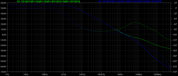
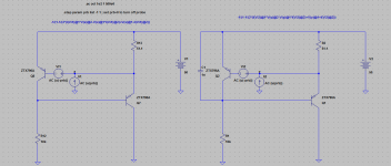
To further enhance stability margins in the ANF current source, a 2k2 resistor in series with the base of the control transistor is shunted by a 10pF~22pF capacitor as shown below.
The capacitor introduces a zero close to the unity loop gain frequency; this increases phase margin from 83 degrees (blue trace) to 114 degrees (green trace).
Attachments
Hi manso,
Do you mean the 30-year-old MOSFET power amp with error correction?
If so, people have asked over the years, but I have never gotten around to it. It was only a 50W amp anyway, so I'm not sure how many would be interested in that low power level.
As an interesting aside, around 1983 I began working on a 200 watt version of it and even had a prototype working, but had to drop it as work demands became intense due to the ATT divestiture and my move from Bell Labs to Bellcore. I recall at the time I was not able to get the P and N channel Hexfets in anything larger than the TO-220 package, so making a high-power amp was painful.
Much later, of course, Halcro took that path and carried the mantle of MOSFET power amplifiers with error correction (the circuit in one of their patents looks remarkably similar).
Cheers,
Bob
Bob maybe you could ask one of the members here to produce a board and you could just evaluate it and oversee. I believe 50 W is ample for normal listening levels inside a home; looking at comercial sector it is around this power level that sales are highest.
It is also the power level where the development of chip amps has shown the greatest advances.I believe 50 W is ample for normal listening levels inside a home; looking at comercial sector it is around this power level that sales are highest.
Bob, someone mentioned that you had done an enhanced chip amp .. or is that wishful thinking on my part?
My personal feeling is 200W @ 8R with nearly twice that into 4R, is sensible for high quality home use with the best speakers. It doesn't guarantee no clipping .. especially if you record 'real life' stuff on the side. But the clipping is likely to be short and infrequent enough to be unnoticeable if the amp behaves when overloaded.
If I was going to the trouble to design & make another amp for myself, that's what I'd be aiming for.
jFET cascode
The k389 & k246 are both 50Vds
Borbely uses the k246 extensively in his designs.
Pass frequently comments that the k170 can be run at it's maximum Vds and even above.
I wonder if the k246 can similarly be run @, or just above, 50Vds?
Could any of the small Zetex mosFETs be used as cascodes for the input stage?
All my jFets have max Vds from 25V to 50V...............It's good for 50W amps and may ju..ust do 200W @ 4R. If anyone has ideas for suitable small signal FETs in this position for big amps, please post. FET i/ps seem to benefit most but BJT i/ps have the edge of THD in my simple amp...............
The k389 & k246 are both 50Vds
Borbely uses the k246 extensively in his designs.
Pass frequently comments that the k170 can be run at it's maximum Vds and even above.
I wonder if the k246 can similarly be run @, or just above, 50Vds?
Could any of the small Zetex mosFETs be used as cascodes for the input stage?
Closed Loop Response to Zillion MHz?
Bob, one of the best bits in your book is the chapter on measurements including the list of test equipment that might be usefully obtained on eBay.
It shows the measurement of various distortions using soundcards is now possible for impecunious beach bums who are versed in the art. (Certainly, emerging from the bush this Millenium, I can now measure speakers & mikes ... more accurately in my shed than I could in Jurassic times with anechoic chambers and (then) SOTA gear.)
But one thing that has come out of this thread is the usefulness of measuring the Closed Loop response of amps to Zillion MHz.
In your 2nd edition, could you perhaps expound a little on how to do that simply and cheaply.
Thanks for these Andrew. When you say 'my jFets' does that mean you have good SPICE models for these?All my jFets have max Vds from 25V to 50V.
The k389 & k246 are both 50Vds
Borbely uses the k246 extensively in his designs.
Pass frequently comments that the k170 can be run at it's maximum Vds and even above.
I wonder if the k246 can similarly be run @, or just above, 50Vds?
Could any of the small Zetex mosFETs be used as cascodes for the input stage?
I think we can juu..ust use these with a following wind, for 200W @ 4R. But 200W @ 8R which I mentioned in post #3508, would need about +/- 70V rails like Toni's excellent 2stageef-high-performance-class-ab-power-amp-200w8r-400w4r
They have to be depletion mode FETs too. High Idss is good to allow the LTP BJTs some Vce to breath.
IIRC, Scott Wurcer mentioned some suitable MOSFETs in the discrete-opamp-open-design thread but I don't think any of them are 70Vds
I just have a small stock of devices, no models..............
IIRC, Scott Wurcer mentioned some suitable MOSFETs in the discrete-opamp-open-design thread but I don't think any of them are 70Vds
The last link takes me to post1.
Where do I see SW's suggestions?
My Leach clone does 170W into 8r0 from a 40+40Vac transformer giving +-58.5Vdc. Although not designed to be capable of driving 4ohms speakers it gets ~310W into 4r0. It is capable of driving 6ohms speaker.
I would expect a 42Vac to 44Vac transformer to achieve at least 200W into 8r0.
When designed to deliver current well, it should just about be able to hit a target of 400W into 4r0.
I would expect a 42Vac to 44Vac transformer to achieve at least 200W into 8r0.
When designed to deliver current well, it should just about be able to hit a target of 400W into 4r0.
But one thing that has come out of this thread is the usefulness of measuring the Closed Loop response of amps to Zillion MHz.
In your 2nd edition, could you perhaps expound a little on how to do that simply and cheaply.
I used to think that any requirement to measure past my 10MHz 'scope limit was just the usual audio fanatic delusional rant.
Now I want at least a 200Mhz scope and oscillator, if not a Vector Network Analyser.
Is there a cheaper way?
Best wishes
David
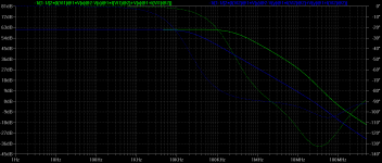
It would appear A&R Cambridge were concerned about instability in the amplified negative feedback (ANF) current source in their A60 amplifier.
They used a 1nF capacitor shunting the collector of the control transistor of all their ANF current sources instead of using a resistor in series with the base of the control transistor:
http://www.retrohifi.co.uk/a60_amp_service_manual.pdf
I simulated the ANF current source loop gain with the 1nF shunt capacitor across the collector of the control BJT and it does indeed reduce loop gain at high frequencies by introducing a dominant pole at about 20KHz.
The blue trace gives the loop gain with the shunt capacitor, while the green trace gives the loop gain without the capacitor.
Attachments
Bob,
For a long time I have been promising some feedback on your book. I will PM you a list of typos but there's other feedback which I imagine may stimulate further discussion/be of interest to everyone so I shall post it here:
page 19, the section on Early Effect states that if the curves in fig. 2.1 are extrapolated back to the x-axis, they will all intersect at the Early Voltage. Strictly speaking this would only be true for all transistors if the parameter for figure 2.1 was Vbe rather than Ib (see for example Analysis and Design of Analog Integrated Circuits 5th Edition International Student Version by Gray, Hurst, Lewis and Meyer, page 15).
page 72 - no mention of how adding further output devices will degrade phase margin (although this is mentioned later on page 212). Also, the 2SC3503/2SA1381 pair has been discontinued by Sanyo; fortunately Fairchild continue to manufacture the identically specified KSC3503/KSA1381.
page 201 - you should mention that in order to minimise inductance, outward and return current paths must enclose as small an area as possible - "non inductive" resistors standing up perpendicular to the board can actually have a higher than expected effective parasitic inductance.
Thermal stability of output stage bias setting
In several places in the book, you mention mounting of Vbe multiplier transistor onto output heatsink, but mounting directly to backside of output transistor is better, as both you yourself note in the book and Douglas Self mentions in his book.
Matched-pair devices for input stage
Are you familiar with the SSM2212 and SSM2220 matched low-noise NPN/PNP pairs from Analog Devices? I've never used them but the specifications look good and they probably deserve a mention in your book (Vce is low and Ccb is high so cascoding is highly recommended)
Output devices in your BJT-output amplifier examples
In the majority of the BJT-output amplifiers in your book, you use very slow transistors in the output stage, both for the drivers and the final output devices. This in turn imposes severe limitations on ULGF and therefore audio-band loop gain. Additionally, these slow devices tend to have other poor attributes such as high levels of "beta-droop". I can't help thinking that perhaps you've done this to make MOSFET-output amplifiers look better? Given the low cost and high performance of ON's MJL1302/3281 etc. pairs, I don't know why you don't just use those in all your BJT-output amplifier examples. Also, try the Fairchild KSA1220A/KSC2690A pair as drivers (Toshiba 2SA1930/2SC5171 are better but are to be discontinued).
PSRR
Please could you add more about PSRR, especially how different compensation techniques will result in different PSRR.
PCB layout and grounding
In the sections on PCB layout and grounding, I feel that these would benefit from significantly more diagrams - pictures here are much easier to understand than written description, with less possibility for misinterpretation. For distribution of the amplifier's power rails, you should explain that if you twist/interleave +/-, this doesn't "cancel" the magnetic field. Rather, magnetic field is still generated, but now it's "linear" (much reduced harmonic content). Also, note that a loudspeaker load will lead to non-linear currents even with a linear output voltage so the most important thing is to minimise efficiency of radiation (out and return paths twisted together) (I do not believe that I have ever seen anyone make this observation before - this is a potential source of distortion in audio power amplifiers when driving real-world loads rather than the usual test-bench resistor. Further investigation is required. Has anyone any references for this?).
Loop-gain simulation
I'd like to add to the previous requests that you cover loop-gain simulation in more depth, including how to set up proper Middlebrook Probe simulations.
Graphs
This is a subjective thing but personally I'd like to see gridlines on all your graphs.
Counterfeit devices
I think it would be worth mentioning the existence of counterfeit devices and the problems they create. Also provide advice on how to avoid buying them and how you could verify if devices you have bought are genuine.
solid-state relays
Please add discussion of solid-state-relays to the section on relays. Modern 150 V rated MOSFETs have low-enough Rdson that distortion is probably lower than standard relays, not to mention all the other benefits of solid-state. Bonsai has a good article on solid-state relays on his hifisonix website.
Balanced input stages
Please could you add a lot more discussion of balanced input stages, including quantification of distortion performance and more options that don't use JFETs (hard to source).
Class-D
Are you familiar with Bruno Putzey's "A universal grammar of class D amplification"? This is a useful reference. A PDF is available from Hypex's website, and an audio recording of a presentation to the AES is available in the AES member section.
Switching loss not accurately described. You refer to the losses incurred in driving the gate of the device as "switching loss", but the term "switching loss" is more normally reserved for the losses incurred as the power device traverses the linear region when switching from the "on" state to the "off" state or visa-versa. During these periods, Id and Vds can be simultaneously large, resulting in instantaneous device power dissipation of several hundred W. Fortunately the switching transients only last a few 10s of nano-seconds.
Driving the gate is usually a lossy process because the traditional technique used is to drive the gate with a voltage source (gate driver) via a resistor. As the gate's capacitance is repeatedly energised/de-energised, power is dissipated in the gate driver's output resistance, the gate resistor and the MOSFET's internal gate resistance. However, the gate capacitor is a fairly high-quality (low-loss) capacitance and there is no inherent need for the energising/de-energising of this capacitance to be a lossy process. If resonant techniques are used, the energising, de-energising, or both, stages of driving the gate can be made a closer-to-lossless process. Please see A First Approach to a Design Method for Resonant Gate Driver Architectures.
Harry, can you send me a copy of the above paper? Thanks.
Bob maybe you could ask one of the members here to produce a board and you could just evaluate it and oversee. I believe 50 W is ample for normal listening levels inside a home; looking at comercial sector it is around this power level that sales are highest.
Good point about 50W. Doing the board is probably the easiest part. Resurrecting the design (clearing my cobwebs), putting in newer parts, and testing/evaluating is where most of the work is. But I'm not saying I won't do it at some point...
.Cheers,
Bob
It is also the power level where the development of chip amps has shown the greatest advances.
Bob, someone mentioned that you had done an enhanced chip amp .. or is that wishful thinking on my part?
My personal feeling is 200W @ 8R with nearly twice that into 4R, is sensible for high quality home use with the best speakers. It doesn't guarantee no clipping .. especially if you record 'real life' stuff on the side. But the clipping is likely to be short and infrequent enough to be unnoticeable if the amp behaves when overloaded.
If I was going to the trouble to design & make another amp for myself, that's what I'd be aiming for.
Hi kgrlee,
Yes, I did what might be called an enhanced chip amp that I called the "Super Gain Clone", based on the LM3886 IC. There is a brief description of its features on my web site at CordellAudio.com - Home under the power amplifier tab. It includes a DC servo and no electrolytics in the signal path, and also has an adaptive soft clipping circuit that I call the "Klever Klipper".
Many of the details of the amplifier are discussed in Chapter 27 of my book. The Klever Klipper is described in Chapter 17.
I also like the 200 wpc power level. One of my favorite small speakers I built is a three-way design with Morel drivers. Its sensitivity is only about 83dB 8ohms. It likes a 200 wpc amplifier on music with good dynamic range and high crest factor. At times, even a 200 wpc amp will clip into these speakers on something like the Ricky Lee Jones cut from Flying Cowboys called "Ghetto of My Mind" played at realistic (but not uncomfortable) levels. Amplifiers do most certainly clip!
Cheers,
Bob
- Home
- Amplifiers
- Solid State
- Bob Cordell's Power amplifier book