Hi Mike,
At what frequency was the peaking, and how much peaking was there.
I assume this was at the output of the amplifier. Dis you look at peaking at the collector of the VAS?
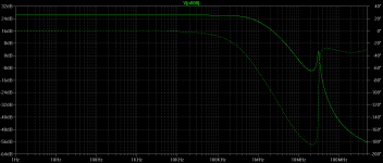
The closed loop frequency response peaking was at 30MHz at the output of the amplifier as shown below. The response at the output of the TIS was virtually identical. As noted previously, you need at least 220pF shunt capacitance at the output of the three transistor TIS to eliminate the peak.
I used Zetex models for the input stage and the TIS. These are also attached, together with the models for the drivers and the output stage; you can compare them with your models.
Attachments
Last edited:
Hi Bob,
How safe would you say it is to rely on spice simulation compared to results from real world circuits? On a percent scale.
Cheers,
My experience tells me that it is not safe to rely on either one by itself. Not sure if this translates to 50%.
Here's why I say this. There is nothing fundamentally wrong with SPICE, insofar as what it models and the reasonableness of its models. However, SPICE does not model everything, such as parasitic inductances in the real world.
On the other hand, unless you do exceptionally detailed measurements on the prototype in the lab, you often may not know how much margin you have against instability. Or even the capacitance of your 10:1 scope probe might be enough to stop an oscillation.
On the positive side, SPICE lets you carry out many, many experiments and lets you look non-intrusively at all the nodes in the circuit (and it lets you easily see signal current as well).
On the positive side for the lab, you are seeing the amplifier in all of its non-ideal, parasitic glory, just as the end user will see it.
I have been implicitly assuming that your question here has to do with safety against instability.
Cheers,
Bob
A french chap in the link below describes his trials and tribulations when he tried the cascoded beta enhanced TIS; I am not sure about his "memory distortion" though:
Memory Distortion Philosophies - Part 8 : More tests
More on "memory distortion":
Lavardin Technologies High End Audio Systems - Technologies
Hi Mike,
Previously called thermal distorsion and firstly addressed to the input stage, this interesting idea has never been given irrefutable proofs for closed loop amps by its author, Hephaïstos - Gérard Perrot who explained his concepts in french "L'Audiophile" (all the following links are in french, however the results do not need to understand it a lot) :
L'tage d'entre de l'amplificateur -1- : tude thorique (Hphatos)
L'tage d'entre de l'ampli : -2- le diffrentiel classique (Hphastos)
L'tage d'entre de l'ampli -3- diffrentiels insolites (Hphastos)
L'tage d'entre de l'ampli -4- exprimentations complmentaires (Hphastos)
My own experiments using voltage followers at 4 Vrms did not show significative changes of distorsion components due to varying thermal conditions of the input stage.
Here are some results with standard DIL op-amps and then with a Shlotzaur configuration :
Distorsions peu connues des étages d'entrée des amplis
.
Last edited:
Only works if you then model everything in the environment as well: real power supplies, real loads, real interference effects. As soon as you include some further reaching, practical aspects to the world of the simulation, everything changes ...Hi Bob,
How safe would you say it is to rely on spice simulation compared to results from real world circuits? On a percent scale.
Cheers,
Michael, I don't understand your reluctance to sim Bob's circuit as is.As I have already noted, I have simulated the circuit with the emitter resistor and found that although it reduces minor loop transmission, it does not improve stability margins, and, indeed, worsens them in this case.
The cross-coupled capacitors in the drivers are not irrelevant; they help expedite the extraction of charge from the output stage as Andy_C demonstrated many years ago. Admittedly, they shouldn't be larger than 1uF, but, in any case, they do not affect minor loop transmission in any way.
Your three transistor TIS remains unstable even when a unity gain ideal VCVS is used for the output stage.
At the moment, you have demonstrated that you can take a working sim of a working circuit with good performance, make substantial changes to it that you think are trivial ... but everyone else thinks important ... and not surprisingly muck it up completely. I'm not sure this is useful

________________
BTW, when I try & run your .ASC file with your BJT_models.txt, the sim craps out with 'Fatal Error: Analysis Failed: Matrix is singular'
If I remove one of the circuits, it still does the same thing.
Any suggestions on how to run your sim to completion? I really want to see for myself the effects you report ... so I'm using your models etc.
________________
Michael, many of use feel that the ONLY reason we do sims is cos they help us get a handle on 'real life'.Perhaps your transistor models are at fault?
On that basis, Bob's models are some of the best around ... though I'm sure even Bob will have caveats. If a sim shows results response/THD/stability that sorta reflects 'real life', I would guess the .ASC & models are probably good.
However, if a sim with certain models is very different from 'real life' then either the .ASC and/or the models does not reflect 'real life'. On that basis, they are 'at fault'.
Sometimes a sim may show results that go against your own theories & prejudices. If you check this in 'real life' and find the sim is 'correct', you have learnt something new & valuable. I have been lucky enough to have had some experiences like this with sims.
But if I may repeat myself, 'Sims/theory are done only cos we hope they reflect real life. If a sim doesn't, it is a bad sim and useless.' It's the theory/sim that has to fit 'real life' ... not the other way round.
Last edited:
My experience tells me that it is not safe to rely on either one by itself. Not sure if this translates to 50%.
Here's why I say this. There is nothing fundamentally wrong with SPICE, insofar as what it models and the reasonableness of its models. However, SPICE does not model everything, such as parasitic inductances in the real world.
On the other hand, unless you do exceptionally detailed measurements on the prototype in the lab, you often may not know how much margin you have against instability. Or even the capacitance of your 10:1 scope probe might be enough to stop an oscillation.
On the positive side, SPICE lets you carry out many, many experiments and lets you look non-intrusively at all the nodes in the circuit (and it lets you easily see signal current as well).
On the positive side for the lab, you are seeing the amplifier in all of its non-ideal, parasitic glory, just as the end user will see it.
I have been implicitly assuming that your question here has to do with safety against instability.
Cheers,
Bob
Hi Bob ,
Spice is certainly a valuable tool as you mentioned.
The reason I asked this is because it seems there is a lot argument going on here in this thread which appears to be solely based on spice simulation. I wonder if anyone has proven the arguments with real world circuits. Considering the differences in component models, the lack of parasitic effects in spice etc. it's a necessary step to construct a real world circuit and test it. I think spice should be used to solve real world circuit problems rather than just perfecting a perfect spice model of the circuit.
This is how I see Douglas Self using spice.
With all the work I've been doing with ultra low distortion oscillators I have not found spice to be not very useful at all. It generates a perfect state variable filter but does not show the Q enhancement effect due to bandwidth limitation of the amplifiers used.
This information is necessary to properly compensate the SVO.
When I use the word safe I'm referring to a danger of over confidence of spice circuits.
Manufactures offer free spice software to sell parts. That's what we find in their libraries. Their parts.
Yes a 10:1 probe can damp an oscillation but in my experience it can just as easily cause it.
This is all very general and not to do with you.
Cheers,
The closed loop frequency response peaking was at 30MHz at the output of the amplifier as shown below. The response at the output of the TIS was virtually identical. As noted previously, you need at least 220pF shunt capacitance at the output of the three transistor TIS to eliminate the peak.
I used Zetex models for the input stage and the TIS. These are also attached, together with the models for the drivers and the output stage; you can compare them with your models.
Hi Mike,
Thanks for providing this closed loop response.
You certainly have demonstrated a fairly sharp peak in the closed-loop response above the ULGF.
But this is not my amplifier.
Please sim this with the component values in my design, if not with the transistors and models I used.
You have made several changes to the design which can influence behavior. You have much higher transconductance in the LTP and correspondingly higher Cm of 100pF. Please use my Cm design value of 30pF. Please use the operating currents that I have used in the LTP and the same degree of degeneration in the mirror. You are running much higher current in the EF preceding the VAS transistor. Please use the amount that I use. Please use emitter degeneration on the VAS transistor, the same value I have.
Once you have done this, it is also a good idea to do a sanity check on the role played by the cascode by seeing what results you get by removing the cascode transistor.
It is significant that you have demonstrated this behavior in a Darlington cascode VAS, but it is also important to demonstrate whether this serious peaking behavior occurs in my circuit.
It is also significant, and in fact somewhat reassuring, that you have shown that in fact this local instability does indeed show up in the closed loop response.
Cheers,
Bob
Not that I really know what I am on about... Please bear in mind I am only a beginner with these things.
But I have a circuit I am simulating with at present using Bob's transistor models and a 3 transistor cascode VAS and this peaking is also present. Only in this case at 35MHz and a 220pF shunt capacitor does crush it and it does show on the amplifier output. Without some sort of shunt RC network the amp oscillates. It's not got a conventional miller cap but even with one the peaking is still present.
Tried changing models and the peak got worse. Is this a feature of the VAS topology or does it imply some strict rules need to be adhered to with these VAS circuits? Next step for me is to try another VAS type to see if the surrounding circuit is the factor.
At least what I am seeing is consistent with what I read here. There's so much to learn.
Of course it exists, the question is to what degree and whether it matters for our purposes. For instance if you depend on the very tight matching of a current mirror without degeneration, thermal modulation could be a significant issue.
I agree completely.
It is interesting that when some mention memory distortion, they don't talk about thermal modulation with program as the cause. Memory distortion as I know it is only caused by program-dependent temperature swings changing amplifier behavior. A simple example apart from transistor die temperature variation would be resistance modulation of the feedback resistor by program-dependent power dissipation in that resistor.
Have people suggested that there are other memory distortion mechanisms than dynamic temperature changes?
I mention memory distortion in connection with output stages in my book on page 234. Here it has to do with program-dependent modulation of the output stage bias current.
Cheers,
Bob
Not that I really know what I am on about... Please bear in mind I am only a beginner with these things.
But I have a circuit I am simulating with at present using Bob's transistor models and a 3 transistor cascode VAS and this peaking is also present. Only in this case at 35MHz and a 220pF shunt capacitor does crush it and it does show on the amplifier output. Without some sort of shunt RC network the amp oscillates. It's not got a conventional miller cap but even with one the peaking is still present.
Tried changing models and the peak got worse. Is this a feature of the VAS topology or does it imply some strict rules need to be adhered to with these VAS circuits? Next step for me is to try another VAS type to see if the surrounding circuit is the factor.
At least what I am seeing is consistent with what I read here. There's so much to learn.
Hi mcd99uk,
Can you share the circuit with us? I'd like to take a look at it.
It is not surprising that a 220pF shunt capacitor at the VAS output crushes the instability, but we'd all prefer that the instability not need that much crushing in the first place. Such a capacitive load at the output of the VAS will generally impair the slew rate ability of the VAS.
As I've mentioned earlier, I do like to use something like a series R-C shunt at the output of the VAS to damp HF goings-on there, especially when an output Triple is being used. In such a network, I'm talking about C values in the 50-100pF neighborhood and R values on the order of 100 ohms or a bit more.
I'll look forward to seeing your circuit, especially since you have elicited some of this behavior using my models.
Cheers,
Bob
Michael, I don't understand your reluctance to sim Bob's circuit as is.
I have simulated Bob's circuit "as is" and still obtain the same results.
I don't know how many times I have to tell you this, but read the following carefully this time: I have simulated the amplifier with the TIS emitter resistor and found that it compromises stability of the minor loop. Your notion that it aids stability is a complete myth in all respects. I hope you don't compel me to repeat this yet again.
Last edited:
I have simulated Bob's circuit "as is" and still obtain the same results.
I don't know how many times I have to tell you this, but read the following carefully this time: I have simulated the amplifier with the TIS emitter resistor and found that it compromises stability of the minor loop. Your notion that it aids stability is a complete myth in all respects. I hope you don't compell me to repeat this yet again.
Hi Mike,
Please attach the .asc and the closed loop response plot.
Cheers,
Bob
I agree completely.
It is interesting that when some mention memory distortion, they don't talk about thermal modulation with program as the cause.
A while ago in the error correction thread you disputed that thermal distortion could be an issue when your error correction transistors are mounted on the heatsink. I agreed as it was evident that such distortion could only exist at very low frequencies and be expressed as an increase in THD at those frequencies.
In respect of the rest of the amplifier, such distortion, if it exists at all, would also exist at very low frequecies. So, why isn't it detectable even in an amplifier of even moderate competence?
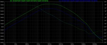
Bob, minor loop phase at unity gain with emitter resistor 192 degrees. (blue trace);
minor loop phase at unity gain without emitter resistor 185 degrees (green trace)
You can do the closed loop frequency response plot yourself if you wish; i've attached the file.
minor loop phase at unity gain without emitter resistor 185 degrees (green trace)
You can do the closed loop frequency response plot yourself if you wish; i've attached the file.
Attachments
Hi Mike,
Please sim this with the component values in my design, if not with the transistors and models I used.
I think I'll leave that to you since I have provided the .asc and the models I used.
Hi mcd99uk,
Can you share the circuit with us? I'd like to take a look at it.
It is not surprising that a 220pF shunt capacitor at the VAS output crushes the instability, but we'd all prefer that the instability not need that much crushing in the first place. Such a capacitive load at the output of the VAS will generally impair the slew rate ability of the VAS.
As I've mentioned earlier, I do like to use something like a series R-C shunt at the output of the VAS to damp HF goings-on there, especially when an output Triple is being used. In such a network, I'm talking about C values in the 50-100pF neighborhood and R values on the order of 100 ohms or a bit more.
I'll look forward to seeing your circuit, especially since you have elicited some of this behavior using my models.
Cheers,
Bob
Bob,
I will gladly share this circuit with you. I'd like to do some more analysis on it first though to confirm that I am getting this peaking in the VAS. It was only last night I looked for it after reading about it in this thread. I saw a peaking at 35MHz and then Mike posted saying that the peak he saw was around 30Mhz.
This amplifier designing is all new to me. Most of the concepts are based on information from your book. Want to be reasonably sure that my circuit is of use to people from an analytical point of view. Don't want to pollute this thread.
I have a habit of going down design "dead ends" and then finding a fundamental floor that I had previously overlooked. This peaking was another example of that. The input filter was masking it...
Paul
Originally Posted by Bob Cordell
Have people suggested that there are other memory distortion mechanisms than dynamic temperature changes?
How about capacitors ? Charge up a cap & then discharge it FULLY, & then watch the voltage rise. Not much i agree, but it does ! Also for eg, sample/hold caps don't retain their voltage forever.
I realise the above examples are pushing the envelope, pun intended, But still "maybe" worthy of consideration ?
A while ago in the error correction thread you disputed that thermal distortion could be an issue when your error correction transistors are mounted on the heatsink. I agreed as it was evident that such distortion could only exist at very low frequencies and be expressed as an increase in THD at those frequencies.
In respect of the rest of the amplifier, such distortion, if it exists at all, would also exist at very low frequecies. So, why isn't it detectable even in an amplifier of even moderate competence?
If an amplifier's THD is dominated by output stage crossover distortion, and the bias of the output stage is influenced by temperature or dynamic temperature mismatching, then its THD may be a function of time as the amplifier warms up or as the amplifier undergoes thermal excursions due to program material. You can see this on a THD analyzer if you measure the THD under idle conditions, then apply 1/3 power for awhile, then eliminate then reduce the audio power level to the level at which THD was measured before. You'll often see the THD change as a function of time under these conditions. Whether this is audible or not is left as a question, but if you believe that the sound of an amp is influenced by how optimum the output stage is biased, then it is plausible.
If an amplifier has been running very hot for some time, getting the heat sink really toasty, and then signal is substantially reduced, the output stage may go through a period of under-bias, since the junction and case temperatures of the output transistors cool down fater than the heat sink.
Cheers,
Bob
- Home
- Amplifiers
- Solid State
- Bob Cordell's Power amplifier book