PMA said:
Really -99dB?
Hi Pavel,
What is your point here? This is just 50 Hz THD that you are showing. I was referring to CCIF 19 + 20 kHz IM when I was referring to seventh order distortion of the JC-1.
Cheers,
Bob
PMA said:Hi Bob,
I thought you was speaking about 7th harmonic of THD.
Anyway, there is just one transfer function, non-linear of course. Based on this non-linear function, it would be possible to derive THD, CCIF IMD and other forms of distortion.
True, but not so easy. I was indeed talking of both 7th THD and 7th order CCIF, and taking some liberty in talking about both in essentially the same breath. I should take that circuit that had only the 34 dB NFB at LF and 20 dB NFB at 20 kHz and simulate it with CCIF for a better comparison.
Cheers,
Bob
john curl said:600W Bob! It would measure better at 60W.
Maybe so, but all I could get my hands on was the numbers in the Stereophile review. It would also be interesting to see how the CCIF turns out at something like 3 V peak, where the crossover distortion might dominate. Based on your high bias and nine output pairs, I'd guess that the crossover distortion is pretty low, however.
I guess you're saying that -99 dB of 7th is OK if it is at very high power, but that it is too high if it is at low power. I suppose that's fair. I guess based on one of your other posts that -114 of 7th is OK no matter what the power. Is that OK?
Cheers,
Bob
john curl said:Optimist!
 I know.
It is a question of math, accurate models, and efficient SW and HW. Once it will be possible quite accurately.
Hi,
Do not calculate...
http://www.hometheaterhifi.com/volume_11_3/parasound-jc1-amplifier-8-2004.html
Do not calculate...
http://www.hometheaterhifi.com/volume_11_3/parasound-jc1-amplifier-8-2004.html
I don´t know, but they used Lynx L22, and you know this measurement,
http://www.hometheaterhifi.com/volume_10_2/bv-audio-pa-300-amplifier-4-2003.html
with same equipment, no mains residuals..
http://www.hometheaterhifi.com/volume_10_2/bv-audio-pa-300-amplifier-4-2003.html
with same equipment, no mains residuals..
PMA said:Anyway, there is just one transfer function, non-linear of course. Based on this non-linear function, it would be possible to derive THD, CCIF IMD and other forms of distortion.
Hi Pavel,
Unfortunately that one transfer function usually changes with time in an unlinear way.
Cheers,
Alex
john curl said:Bob, you are speculating again and with a commercial product. Put up real numbers, or cease and desist.
There was nothing wrong with what I said in my last post. Stop whining. Why don't you just answer the question that was posed in that post?
Bob
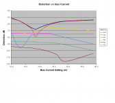
Distortion vs bias current
The plot below shows the crossover distortion spectra as a function of idle bias current for the Class-AB output stage with no negative feedback discussed earlier.
This stage employs the ThermalTrak RET NJL3281D and NJL1302D OnSemi output transistors with the SPICE models developed by Andy_c. Emitter resistors are 0.22 ohms and the load resistance is 4 ohms.
The simulations were done at an output voltage of 3.0 V peak. This is the signal level where this stage creates the most crossover distortion when it is near optimum idle bias. The fundamental frequency is 1 kHz.
In the plot, the idle bias current is expressed as the number of millivolts dropped across each RE.
The top dark bold curve is THD-1 expressed in dB. It has a minima at a bias voltage of 18.5 mV. The orange curve below it is third harmonic. We can easily see that when we optimize the bias for lowest crossover distortion based on THD, we are essentially adjusting for lowest third harmonic.
Note, however, that the next curve down, the yellow curve for fifth harmonic, is actually larger than the nulled third harmonic in the vicinity of the optimum bias. That is why the THD null is not as deep as the third harmonic null.
A look at the seventh harmonic reveals some interesting information. That is the blue curve. Notice that it goes to a null at bias current levels below the “optimum”. This was also suggested in an earlier post above. Great caution is needed here in dealing with the temptation to under-bias the output stage so as to minimize 7th harmonic at the expense of third harmonic. Just look how sharply it rises at bias levels below its minima. This is dangerous territory.
If one is going to try for better high-harmonic performance at the expense of THD and third harmonic, it appears to be wiser to over-bias the output stage. This probably explains why overbiased output stages sound better. As long as thermal stability is not unduly compromised by some over-biasing of the output stage, this appears to be the better side to err on.
Overbiasing to 39 mV “hurts” THD by 14 dB compared to its null.
Overbiasing to 39 mV hurts 3rd by 25 dB compared to its null, but the value at its null is not very useful because the null is fairly sharp.
Overbiasing to 39 mV hurts 5th by nothing net because of the shallow slope of 5th between the optimum bias point and 39 mV.
Overbiasing to 39 mV HELPS 7th by 14 dB compared to the optimum bias point.
What I’ve described here with the plot below is what happens when the user “tweaks” the bias pot with a given design. There is another way to look at this, however. Suppose the designer decides up front to bias the output stage at the 178 mA that corresponds to the 39 mV over-bias situation. Can he now do better, at the same given 178 mA bias current, with a different value of RE? Investigating that would call for a plot of distortion vs RE with Ibias held constant. Maybe I’ll try to take a look at that next week.
Cheers,
Bob
Attachments
Hi Bob,
very nice. If I look at the 7th, your result in mV seems to be similar to mine in
http://www.diyaudio.com/forums/showthread.php?postid=1289633#post1289633
, a point of minimalized 7th.
The case is pretty complex, as for every amplitude of input voltage we get different "optimal" bias for the given harmonic order.
IMHO, it does not make much sense to try to minimalize harmonics of Xth order somewhere. Other methods of design should be used, and they are class A or error correction, or - difference of two squares.
To prevent possible misunderstanding, this is nothing against your simulations. As always, they yield very good example and they are very helpful.
Regards,
Pavel
Re: Distortion vs bias current
Great work! Difficult to minimize Spice after this.
First question wath are the base and emitter parasitic resistance in the model you have used?
According to Oliver's paper and using your data ( 85mA bias optimal) the Worse output voltage ( for distortion) should be a little more than 2 Volts.
An interesting view would be to plot the distortion curves with respect to i/Io where Iload = i+Io with gmRe as parameter.
Nice work
Jean-Pierre
Bob Cordell said:The plot below shows the crossover distortion spectra as a function of idle bias current for the Class-AB output stage with no negative feedback discussed earlier.
This stage employs the ThermalTrak RET NJL3281D and NJL1302D OnSemi output transistors with the SPICE models developed by Andy_c. Emitter resistors are 0.22 ohms and the load resistance is 4 ohms.
The simulations were done at an output voltage of 3.0 V peak. This is the signal level where this stage creates the most crossover distortion when it is near optimum idle bias. The fundamental frequency is 1 kHz.
In the plot, the idle bias current is expressed as the number of millivolts dropped across each RE.
The top dark bold curve is THD-1 expressed in dB. It has a minima at a bias voltage of 18.5 mV. The orange curve below it is third harmonic. We can easily see that when we optimize the bias for lowest crossover distortion based on THD, we are essentially adjusting for lowest third harmonic.
Note, however, that the next curve down, the yellow curve for fifth harmonic, is actually larger than the nulled third harmonic in the vicinity of the optimum bias. That is why the THD null is not as deep as the third harmonic null.
A look at the seventh harmonic reveals some interesting information. That is the blue curve. Notice that it goes to a null at bias current levels below the “optimum”. This was also suggested in an earlier post above. Great caution is needed here in dealing with the temptation to under-bias the output stage so as to minimize 7th harmonic at the expense of third harmonic. Just look how sharply it rises at bias levels below its minima. This is dangerous territory.
If one is going to try for better high-harmonic performance at the expense of THD and third harmonic, it appears to be wiser to over-bias the output stage. This probably explains why overbiased output stages sound better. As long as thermal stability is not unduly compromised by some over-biasing of the output stage, this appears to be the better side to err on.
Overbiasing to 39 mV “hurts” THD by 14 dB compared to its null.
Overbiasing to 39 mV hurts 3rd by 25 dB compared to its null, but the value at its null is not very useful because the null is fairly sharp.
Overbiasing to 39 mV hurts 5th by nothing net because of the shallow slope of 5th between the optimum bias point and 39 mV.
Overbiasing to 39 mV HELPS 7th by 14 dB compared to the optimum bias point.
What I’ve described here with the plot below is what happens when the user “tweaks” the bias pot with a given design. There is another way to look at this, however. Suppose the designer decides up front to bias the output stage at the 178 mA that corresponds to the 39 mV over-bias situation. Can he now do better, at the same given 178 mA bias current, with a different value of RE? Investigating that would call for a plot of distortion vs RE with Ibias held constant. Maybe I’ll try to take a look at that next week.
Cheers,
Bob
Great work! Difficult to minimize Spice after this.
First question wath are the base and emitter parasitic resistance in the model you have used?
According to Oliver's paper and using your data ( 85mA bias optimal) the Worse output voltage ( for distortion) should be a little more than 2 Volts.
An interesting view would be to plot the distortion curves with respect to i/Io where Iload = i+Io with gmRe as parameter.
Nice work
Jean-Pierre
PMA said:Hi Bob,
very nice. If I look at the 7th, your result in mV seems to be similar to mine in
http://www.diyaudio.com/forums/showthread.php?postid=1289633#post1289633
, a point of minimalized 7th.
The case is pretty complex, as for every amplitude of input voltage we get different "optimal" bias for the given harmonic order.
IMHO, it does not make much sense to try to minimalize harmonics of Xth order somewhere. Other methods of design should be used, and they are class A or error correction, or - difference of two squares.
To prevent possible misunderstanding, this is nothing against your simulations. As always, they yield very good example and they are very helpful.
Regards,
Pavel
Thanks, Pavel. I agree. If anything, these plots show the complexity of the beast and the difficulty of making a good compromise on the bias point setting. Indeed, if I had done these plots at a higher or lower signal level, things might have been different.
I do also agree that this makes a good case for the use of error correction.
I would also point out, however, that the use of a larger number of output pairs (with a consequent increase in total idle bias current) can be expected to reduce these crossover levels in proportion.
For example, I would guess that if we went to four output pairs and 4X the idle current, all of the curves on my plot would drop by about 12 dB. Of course, if we did that, and used the 39 mV over-bias end of the plot, we'd have a very healthy total idle bias of about 700 mA. The 7th would then be down to perhaps -102 dB WITHOUT NFB - not bad. If that amp had 70V rails, it would have an idle dissipation of about 100 Watts. It would also have a quasi-Class-A region into 8 ohms up to nearly 8 watts.
Cheers,
Bob
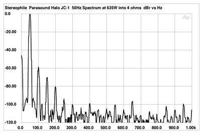
Fellow designers, I would like to explain how I check my Parasound amps for minimum distortion.
First of all, I don't think that extremely high output levels are the most realistic place to evaluate an amp. Usually I chose an output level that will just show any significant distortion change, especially of higher order products. This is usually slightly above the rated class A region of the amp.
So, in the case of the JC-1:
It is typically operating about 25W class A into 8 ohms, so I might operate it at 25-50W into 4 ohms. This insures that I am in the class B region, and 4 ohms is always worse than 8 ohms in my amps.
I then set my Sound Technology 1700B to 5KHz, put a passive filter on the output of the oscillator (thanks Scott Wurcer for that tip many years ago) and get a measurement of my amp into a 4 ohm load operating between 25-50W or so, wherever I can find a worse case in the region. I get a THD null from the Sound Technology and I run it into my HP 3563 FFT analyzer to do a FFT of the results. I usually measure about 115dB down with the 7th harmonic (35KHz) in this case.
Personally I don't care much if the harmonic distortion, including 7th harmonic distortion tends to increase after 400W or so. It just has to meet THX, and there isn't much that I can do about it anyway, except to add some form of negative feedback. I don't like further stage complexity, so I tend to not do this.
For the record, please note the same distortion done by 'Stereophile' measuring the Halcro. It might be somewhat informative in this case.
Bob Cordell said:
For example, I would guess that if we went to four output pairs and 4X the idle current, all of the curves on my plot would drop by about 12 dB. Of course, if we did that, and used the 39 mV over-bias end of the plot, we'd have a very healthy total idle bias of about 700 mA. The 7th would then be down to perhaps -102 dB WITHOUT NFB - not bad. If that amp had 70V rails, it would have an idle dissipation of about 100 Watts. It would also have a quasi-Class-A region into 8 ohms up to nearly 8 watts.
Cheers,
Bob
Hi Bob,
this is a good point (and imagine if they were nine!!
).Greater number of output devices would also allow them to work in an area where hFE does not drop that much with Ic.
Regards,
Pavel
john curl said:
It is typically operating about 25W class A into 8 ohms, so I might operate it at 25-50W into 4 ohms.
Wrong. If you operate class AB till 25W/8 ohm in class A, it would be only 12.5W/4 ohm in class A.
The formula for class A in push-pull is Pa = (4 x I(q) x I(q) x Rload) / 2.
- Home
- Amplifiers
- Solid State
- Bob Cordell Interview: Negative Feedback