")
mikeks said:
The problem with this, i suspect, is clipping in the input stage (current swing entirely from one transistor to the other) is not necessarily related to voltage clip in subsequent stages.
Mike, it depends on the input stage circuitry. I was only referring to the input stage and VAS interconnection in my published MOSFET power amplifier on my web page as an example. In that circuit, the cascoded differential input stage is loaded with a special differential current source that has very high impedance differentially and low impedance in the common mode. If the input differential pair cannot correct for an input-output anomoly, the difference voltage at those collectors will quickly go to +/- 1 diode drop, and some current will flow in the catch diodes (which can easily be detected if the diodes are replaced with transistors). The input differential pair does not have to be railed, current-wise, for this to happen.
Of course, your results will vary if you try this technique with other types of input differential pairs.
Bob
Hi Bob,
-Chris
True, but by virtue of how a differential pair works, you will an unbalance. I would think that another diff pair in parallel could detect this rather easily, or you could move the detection within the circuit as you suggested.Of course, your results will vary if you try this technique with other types of input differential pairs.
-Chris
Bob Cordell said:
Mike, it depends on the input stage circuitry. I was only referring to the input stage and VAS interconnection in my published MOSFET power amplifier on my web page as an example. In that circuit, the cascoded differential input stage is loaded with a special differential current source that has very high impedance differentially and low impedance in the common mode. If the input differential pair cannot correct for an input-output anomoly, the difference voltage at those collectors will quickly go to +/- 1 diode drop, and some current will flow in the catch diodes (which can easily be detected if the diodes are replaced with transistors). The input differential pair does not have to be railed, current-wise, for this to happen.
Of course, your results will vary if you try this technique with other types of input differential pairs.
Bob
Hi Bob,
You're were absolutely correct. You may have noticed i stated somewhere earlier that i have no experience with this sort of circuitry.
Just trying to sort things out in my own mind in order to establish THE optimum approach before i construct anything.
Cheers.
i agree upupa:
i am more interested in knowing the amp is nearing onset of clipping versus knwoing that clipping has actually occured.
mlloyd1
i am more interested in knowing the amp is nearing onset of clipping versus knwoing that clipping has actually occured.
mlloyd1
Upupa Epops said:...Better is indicator, which indicate level - 1 dB ( or 3 dB - it is free) below clipping....
mlloyd1 said:i agree upupa:
i am more interested in knowing the amp is nearing onset of clipping versus knwoing that clipping has actually occured.
mlloyd1
This is fine as long as you realize that if the amplifier runs out of current, that condition will not be indicated with this approach.
Bob
mikeks said:
Don't be too hard on yourself old chap.
Actually I'm not that old and I'm only hard on myself when I believe I'm wrong.
To be old I'd have to be repeating others endlessly, going over the same ground looking for something, and spend my days polishing doorknobs because I didn't know what else to do with them.
Regards, Mike.

mikeks said:
You're right about the input error voltage-i misunderstood Chris.
As for the current peaks, you may have a point: after all an anomalous increase in error voltage must necessarily lead to an accompanying increase in current in one or other of the Diff. stage BJTs.
Any concrete ideas in respect of circuitry?
I've not tried this one, but it is one example:
http://sound.westhost.com/project57.htm#top
Bob's suggestion of what is essentially a null test is good also but you have to compensate for the amp transfer function. Here it is:
http://sound.westhost.com/sim.htm
I agree that any of these should have a one shot, to provide a long enough pulse to the LED so that it is visible.
The Adcom GFA-555 I think it is has a very simple circuit around the VAS as a clipping indicator, don't remember the details.
Pete B.
mikeks said:However, if the intention is to monitor the input error voltage (red trace) for unusually large spikes, then, as Bob has pointed out, this may be a workable approach.
Did you notice the blip in both the red and blue traces at the end of the clipping period on the positive output waveform but not the negative. Have you expanded that blip along the time scale? I'd expect that it looks like ringing from what I've seen in simulation.
Pete B.
Hi Pete,
-Chris
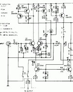
Right you are, sort of. It's triggered right in the diff pair. The collector of Q2 draws enough current to trigger Q5 and light L1. See attached schematic. It's assumed for an AC signal, a DC fault in the wrong polarity would not light the lamp. Close enough for rock 'n roll!The Adcom GFA-555 I think it is has a very simple circuit around the VAS as a clipping indicator, don't remember the details.
-Chris
Attachments
Non-complementary input differential pairs
Hi Tony,
I'll now try to answer your second very good question. My input circuit is not fully complementary in the sense that I do not use two input differential pairs, one npn and one pnp. However, my input and VAS circuits are fully differential, not single-ended. Take a look at the input stage/VAS circuit in my MOSFET power amplifier on my web site at www.cordellaudio.com.
That circuit uses an N-channel JFET input differential pair that is cascoded. Both collectors of the cascode are loaded by a differential current source that has a low common-mode impedance. Those collectors then drive a cascoded pnp differential pair that is the top part of the VAS. One output of that cascode drives the output stage. The other output goes down to a cascoded NPN current mirror, whose output also drives the output stage. Thus, the whole thing is differential and push-pull.
Your real question is probably why I did not go with a symmetrical topology like the one so many people use with complementary input differential pairs. Obviously, mine is asymmetrical (but that does not mean it is single-ended).
The popular architecture using complementary differential pairs looks clever and symmetrical and elegant on paper, and it radiates a kind of synergy to the eye. It looks cool. People like visual symmetry, and are inclined to believe that it must perform better. I did not follow the crowd on this one. I assure you, if I thought it would perform better, I would have used it.
Unfortunately, there seems to be no good way of using current mirrors to load each of the complementary differential pairs the way that we would load a single differential pair. If you try it (and at least one author has), you will find that the standing current in the VAS stage is not well defined. For that reason, most designs I've seen that use this topology resistively load the differential pair. This sacrifices current balance in the differential pair and gain. Many good amplifiers have been made using this architecture, but the designers have generally had to accomodate this limitation in one way or the other.
The asymmetrical balanced differential design I use provides superior performance and does not end up costing much more, if anything. It also affords me greater freedom in selecting the most desirable single-sex matched input differential pair device.
Cheers,
Bob
Tony said:Hi Bob,
i know that J Curl and Leach favor bipolar output transistors as opposed to you favoring mosfets, care to elaborate on this?
again, your circuits seem to be single ended at input and VAS stages, am i correct or do you have any design that is fully complimetary from input to output?
thanks..
Hi Tony,
I'll now try to answer your second very good question. My input circuit is not fully complementary in the sense that I do not use two input differential pairs, one npn and one pnp. However, my input and VAS circuits are fully differential, not single-ended. Take a look at the input stage/VAS circuit in my MOSFET power amplifier on my web site at www.cordellaudio.com.
That circuit uses an N-channel JFET input differential pair that is cascoded. Both collectors of the cascode are loaded by a differential current source that has a low common-mode impedance. Those collectors then drive a cascoded pnp differential pair that is the top part of the VAS. One output of that cascode drives the output stage. The other output goes down to a cascoded NPN current mirror, whose output also drives the output stage. Thus, the whole thing is differential and push-pull.
Your real question is probably why I did not go with a symmetrical topology like the one so many people use with complementary input differential pairs. Obviously, mine is asymmetrical (but that does not mean it is single-ended).
The popular architecture using complementary differential pairs looks clever and symmetrical and elegant on paper, and it radiates a kind of synergy to the eye. It looks cool. People like visual symmetry, and are inclined to believe that it must perform better. I did not follow the crowd on this one. I assure you, if I thought it would perform better, I would have used it.
Unfortunately, there seems to be no good way of using current mirrors to load each of the complementary differential pairs the way that we would load a single differential pair. If you try it (and at least one author has), you will find that the standing current in the VAS stage is not well defined. For that reason, most designs I've seen that use this topology resistively load the differential pair. This sacrifices current balance in the differential pair and gain. Many good amplifiers have been made using this architecture, but the designers have generally had to accomodate this limitation in one way or the other.
The asymmetrical balanced differential design I use provides superior performance and does not end up costing much more, if anything. It also affords me greater freedom in selecting the most desirable single-sex matched input differential pair device.
Cheers,
Bob
Guys,
given the thread heading you two are quite welcome to read this one too =>
www.multimediamanufacturer.com/articles/Cordell-1206.pdf
given the thread heading you two are quite welcome to read this one too =>
www.multimediamanufacturer.com/articles/Cordell-1206.pdf
Re: Error correction?
Both look like variations of Hawksford's circuits. However I found Hawksford's circuit from Fig.4. in his original paper more inspiring.
(No?)
edit: You will find more EC patents on D.Self's site
mikeks said:
Both look like variations of Hawksford's circuits. However I found Hawksford's circuit from Fig.4. in his original paper more inspiring.
(No?)
edit: You will find more EC patents on D.Self's site
Re: Re: Error correction?
I've found both as additional feedbacks... Hmmm.... May be it is the time to patent Ohm's Law in application to Audio?
darkfenriz said:
Both look like variations of Hawksford's circuits. However I found Hawksford's circuit from Fig.4. in his original paper more inspiring.
(No?)
I've found both as additional feedbacks... Hmmm.... May be it is the time to patent Ohm's Law in application to Audio?
- Home
- Amplifiers
- Solid State
- Bob Cordell Interview: Error Correction