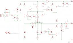
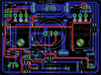
The Amplifier measures the Voltage between Jin1 & Jin2, then scales this difference to present that new voltage at the output (across OUT to PGND)
The INPUT difference signal is compared all the way along the Signal Return trace from Jin2 to bottom of C2 to bottom of R3 to bottom of R6 and measured against the Voltage on the trace from Jin1 to C1 and to C1b and to C1c
This DIFFERENCE should by design be as constant along any part of those long traces as you can possibly make it.
That requires YOU to layout these traces so that they don't pick up interference from other parts of the circuit and from you mobilephone and from the thermostat in your fridge/freezer. Three very different ROUTES for interference entry.
If either of these two traces pick up interference, then the VOLTAGE at one end could/will be different at other points along the trace and at the far end.
The Signal Hot trace and the Signal Return trace must have absolute minimal LOOP AREA.
AND
the Power Ground must not be able to inject it's own interference into the trace.
This final part is where I and others are disagreeing on whether a Signal Return to Power Ground resistor/diode could be useful in minimising injection of interference.
Last edited:
The effect of where C3 connects is not resolved.
If this cap could inject a little bit of interference into the Signal Return trace, then it's effect would be less if it tied into the trace at the END, i.e just to the right of the R6 tie in point.
What might help is splitting R2 and adding in a second C. This extra C would take most of the rail interference into the Power Ground. Then C3 is presented with a "cleaner" rail voltage and the interference that comes out of it's bottom end will also be "cleaner". This could then connect to the right of R6.
Member
Joined 2009
Paid Member
I can't build this without buying the boards. It isn't a complex circuit. Why not single sided?
A single sided board is possible when using through-hole parts like this. Of course asking poor Christian to start over is another thing! I used to make my own boards and I designed them as single sided - I took a few precautions in the layout of the pcb to make home manufacture easier and those tricks would need to be added to the list.
Since the days of staining the laundry sink dark brown and drilling hundred holes by hand I've ordered boards from China. For VERY little money I can get two layer boards with plated through holes, and holes all drilled out. It's a real boon to DIY, the cost is tiny compared with the time saved (we're talking $20 for 10 boards) and the quality is good. You get to do a 'proper' pcb design since you aren't restricted by the kitchen sink method. You get better, more reproduceable results.
the Signal Return is connected to a Power Ground !!!!!
I missed that one.
Last edited:
(we're talking $20 for 10 boards)
Got a link?
I would move the track at C1R1 junction. Your board house might complain. While I'm here, as a DIYer, I can't build this without buying the boards. It isn't a complex circuit. Why not single sided?
As Bigun remarked, it is very inexpensive to have small boards manufactured, and then the second layer is "free" so I might as well use it. Actually, I've never tried to etch my own boards - it just seems like a lot of hassle for a sub-standard result.
The Amplifier measures the Voltage between Jin1 & Jin2, then scales this difference to present that new voltage at the output (across OUT to PGND)
The INPUT difference signal is compared all the way along the Signal Return trace from Jin2 to bottom of C2 to bottom of R3 to bottom of R6 and measured against the Voltage on the trace from Jin1 to C1 and to C1b and to C1c
This DIFFERENCE should by design be as constant along any part of those long traces as you can possibly make it.
That requires YOU to layout these traces so that they don't pick up interference from other parts of the circuit and from you mobilephone and from the thermostat in your fridge/freezer. Three very different ROUTES for interference entry.
If either of these two traces pick up interference, then the VOLTAGE at one end could/will be different at other points along the trace and at the far end.
The Signal Hot trace and the Signal Return trace must have absolute minimal LOOP AREA.
AND
the Power Ground must not be able to inject it's own interference into the trace.
This final part is where I and others are disagreeing on whether a Signal Return to Power Ground resistor/diode could be useful in minimising injection of interference.
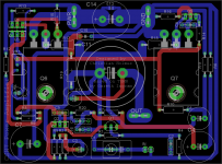
I took care with the grounding but accidentally made a gross error with C7. I see that on this layout that C7 injects directly into SGND and agree that this needs to be fixed as a priority. You're other comments about minimising the loop areas for the different routes: I agree that this is desirable but easier said than done on an already very compact PCB (3 x 4" incl. underslung outputs!). I'll keep looking over the next day or two and see if any further practical improvements can be made.
The effect of where C3 connects is not resolved.
If this cap could inject a little bit of interference into the Signal Return trace, then it's effect would be less if it tied into the trace at the END, i.e just to the right of the R6 tie in point.
What might help is splitting R2 and adding in a second C. This extra C would take most of the rail interference into the Power Ground. Then C3 is presented with a "cleaner" rail voltage and the interference that comes out of it's bottom end will also be "cleaner". This could then connect to the right of R6.
It seems a shame to complicate the design by adding another cap and resistor for something so rudimentary as transistor biasing. I did think about splitting R2, moving C3 to the midpoint with its ground returned to PGND and eliminating R3. So effectively a rearrangement of the components but no new components. Thoughts?
Got a link?
Try PCB.HQEW.net 10 boards cost me around US$23 provided the dimensions are kept within 10x10cm.
Last edited:
Member
Joined 2009
Paid Member
Member
Joined 2009
Paid Member
Member
Joined 2009
Paid Member
Looking good.
A couple of ideas on the silk screen labels - add some "+" symbols for the electrolytic caps outside of their footprints so that you can check correct polarity after they have been soldered in place. And you could move your name (and mine) from under the main cap and place them over the top of the power devices, then you'll still be able to read them (add a 'pcb version 1.0').
A couple of ideas on the silk screen labels - add some "+" symbols for the electrolytic caps outside of their footprints so that you can check correct polarity after they have been soldered in place. And you could move your name (and mine) from under the main cap and place them over the top of the power devices, then you'll still be able to read them (add a 'pcb version 1.0').
Dear friends,
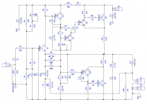
I had been searching my collection of schematics. JLH has not used ground lift transistor nor Dr Bailley nor Bloomley. I had seen Electors Edwin and Equa amps and they do not use this resistor. Only Equin amp uses a 2R2 between VAS and Power stage. So, my use of this resistor is 'over enthusiasm'.
I have corrected the files and uploaded again.
I retained R20 at the input to take care of C1 if it is electrolytic.
I retained R10 the second feedback resistor and R 26 as place holders. Only one of them is necessary.
Split R3 into R3+VR1. The final values are to be frozen.
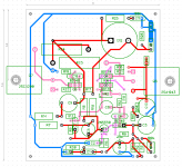
Urgent comment on the layout made in Diptrace are invited. This is the first time I am making a layout. All earth lines from Electrolytics will be connected directly to J4.
Is an output coil required? Left space on the layout.
--gannaji
I had been searching my collection of schematics. JLH has not used ground lift transistor nor Dr Bailley nor Bloomley. I had seen Electors Edwin and Equa amps and they do not use this resistor. Only Equin amp uses a 2R2 between VAS and Power stage. So, my use of this resistor is 'over enthusiasm'.
I have corrected the files and uploaded again.
I retained R20 at the input to take care of C1 if it is electrolytic.
I retained R10 the second feedback resistor and R 26 as place holders. Only one of them is necessary.
Split R3 into R3+VR1. The final values are to be frozen.
Urgent comment on the layout made in Diptrace are invited. This is the first time I am making a layout. All earth lines from Electrolytics will be connected directly to J4.
Is an output coil required? Left space on the layout.
--gannaji
Attachments
Last edited:
Mono amplifiers do not benefit from the added resistor to attenuate the current around the LOOP created with the TWO inputs that don't exist !
It's when TWO amplifiers. or more, are assembled into a multi-channel amplifier that the added resistor is required.
If JLH, Bailey, Blomley and all the Elector amps are discussing the build of a mono, then obviously they won't mention an unnecessary added resistor.
It's when TWO amplifiers. or more, are assembled into a multi-channel amplifier that the added resistor is required.
If JLH, Bailey, Blomley and all the Elector amps are discussing the build of a mono, then obviously they won't mention an unnecessary added resistor.
Final
Thanks guys, have incorporated most of your comments, and sent the files off to the board house a few minutes ago. Looking forward to building this in a few weeks.
Gareth, my numbering schema is a little different you yours. If I respin the same design I add "Rev. 1" (and so forth) to the PCB.
Thanks guys, have incorporated most of your comments, and sent the files off to the board house a few minutes ago. Looking forward to building this in a few weeks.
Gareth, my numbering schema is a little different you yours. If I respin the same design I add "Rev. 1" (and so forth) to the PCB.
Attachments
Member
Joined 2009
Paid Member
I have corrected the files and uploaded again.
I retained R20 at the input to take care of C1 if it is electrolytic.
I retained R10 the second feedback resistor and R 26 as place holders. Only one of them is necessary.
Split R3 into R3+VR1. The final values are to be frozen.
Hi Gannaji,
Some thoughts on your updated schematic file which I hope are helpful:
- I do believe that based on the experience of others, you can eliminate the base-stopper resistors R21 and R22 from your initial build.
- R9 is optional, it provides some local feedback which has been reported to have some benefit on the sound but it's a very subtle thing - you may like to build without R9 at first and then add it later to see if it adds anything good
- C7 is shown as 200p, do you need a value so high ?
- C6, as you know, good to try lower values and find the sound you like best
- VR2 for safety people usually put another fixed resistor in series with it
- C13 could be a much larger value if you have space on the board
Christian - nice looking board - we want to see pics when they arrive
")
Last edited:
Member
Joined 2009
Paid Member
Is an output coil required? Left space on the layout.
I believe an output coil is a good precaution against errant behaviour into difficult speaker loads (and cables). One option that I have used is to leave the output coil off the board and instead I install it in-line, in the wire connecting the amplifier board to the speaker binding posts.
Member
Joined 2009
Paid Member
Urgent comment on the layout made in Diptrace are invited. This is the first time I am making a layout. All earth lines from Electrolytics will be connected directly to J4.
I haven't had much experience of working with perf board but I guess one of the main things is to lay out the parts so that it isn't too difficult to install them and replace them whilst you are experimenting. If you want to experiment it would be really convenient if you can access both sides of the board whilst the power devices are bolted to a heatsink and powered up. This way you can probe voltages anywhere on the circuit easily. And you can replace parts without taking the power devices off the heatsink. If you want to have this flexibility, put the power devices on one edge of the board, standing up, so the board can be perpendicular to the heatsink.
Do you want to have VR1 facing the other direction - it seems that you need to be able to get a screw driver to the adjustment screw and C3 might block access ? Make sure C9 doesn't block a screwdriver to VR2.
For thermal control you may want to put Q3 into direct physical contact with Q4 - I guess you plan to install them tall enough to be above R16 and bend their leads slightly until they touch.
gannaji, that phase lead, C7, is *far* too big; at 200p it will absolutely kill the sound. You will probably find its not required, but if it is start with 10p, 22p, or thereabouts.
Bigun, not sure about your comment re. the trimpot VR2. I sometimes insert a series fixed resistor to limit the adjustment range. However if the wiper goes open circuit, the bias transistor's BC resistance will be infinite, with or without the fixed resistor. To my understanding, we put the trimpot between the BE legs, instead of the BC, so that if/when it does go open circuit, the bias voltage safely collapses instead of having the opposite effect.
Bigun, not sure about your comment re. the trimpot VR2. I sometimes insert a series fixed resistor to limit the adjustment range. However if the wiper goes open circuit, the bias transistor's BC resistance will be infinite, with or without the fixed resistor. To my understanding, we put the trimpot between the BE legs, instead of the BC, so that if/when it does go open circuit, the bias voltage safely collapses instead of having the opposite effect.
Last edited:
- Status
- This old topic is closed. If you want to reopen this topic, contact a moderator using the "Report Post" button.
- Home
- Amplifiers
- Solid State
- Bigun's TGM8 with Single Supply