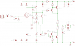
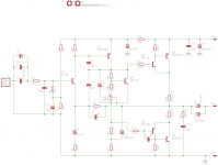
Thanks Andrew, I've fixed up the connections for the input bias voltage divider network, as attached. Values are just placeholders to be determined during testing.
There are three main poles that determine the LF response of this system: the input HP filter, the NFB shunt network, and a third at the output node. The VAS bootstrap also forms a pole that has a secondary contribution to the overall system response. I understand that the cut-off frequency for these three poles should be in descending order, from input to output.
The schematic at #39 puts the output fc at a little over 4 Hz assuming an 8-ohm speaker load. This is not a wonderful place to start if we want to keep the proceeding poles well outside the audible band. The other issue is that I have eliminated the second feedback loop, that had enclosed the output capacitor, out of concern that it will introduce phase shift in the feedback system and error at the summing point. That second feedback loop would have been very effective at reducing LF distortion contributed by the coupling capacitor.
I want to keep the coupling cap on board so I've pushed and pulled the surrounding parts and managed to squeeze in a 30mm pad. Rail voltage is 50V, with about half that voltage across it at quiescent, and about 33Vpk at full power. So a 50V coupling cap provides adequate margin, and 12mF is about the most capacitance I can readily source at that VW rating within the 30mm pad constraint. This gives a new cut-off frequency of 1.7 Hz at the output node - a small but worthwhile improvement, that not only reduces LF distortion but give some flexibility when setting up the proceeding LF poles. A small value, low ESR electrolytic is added in parallel to improve HF response.
Unlike an LTP diff amp, the feedback shunt resistor on a singleton input serves double-duty, adding emitter degeneration, linearising the input stage but reducing loop feedback as a result.
The P3A that Gareth based his TGM8 is based features undegenerated input and VAS stages (miller cap function notwithstanding) with this raw transconductance from these transistors translating to a relatively high OLG for a simple design.
The input filter and NFB network values in my schematic were pretty much copied from Gareth's design and I'd not given this much thought until now. I suspect that Gareth chose an unusually low value (56R) shunt resistor so as to keep the OLG high, in keeping with Rod's P3A design ethos. The issue is that it places the pole quite high at 6 Hz with the 470uF shunt cap specified.
The shunt cap with the necessary 35V rating is already a fairly bulky part so I have opted instead to increase the shunt resistor to 100R. This puts the new fc at 3.4 Hz - or about double that of the output node with an 8R load.
I've committed myself to using a FET input for this project, which are already more linear but have less raw transconductance than the bipolar in the original P3A and TGM8 designs. Instinctively 100R source degeneration feels like the upper limit in terms of balancing local linearity and overall loop gain in this simple design. I feel it is a reasonable compromise however it may be beneficial to push up the drain load or add an extra gain element to increase OLG.
A 1.5uF input coupling cap is chosen to give a new fc of 3.9 Hz. This is uncomfortably high frequency for electrolytic duty so instead I have specified a quality Polypropylene in its place, which should greatly reduce LF distortion generated as the signal passes through the dielectric.
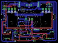
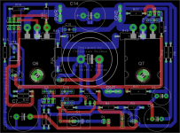
Attachments
OK, thanks Andrew, I investigated further and found the 1mF either 35V or 50V available in a 16mm footprint - smaller than I thought. I worry about RFI pickup with these bigger caps, but I've substituted that part anyway and made a few other changes also, including a JFET in place of the MOSFET input.
gannaji, how is yours coming along?
I'm close to sending this one off to the board house so if anyone has any further suggestions?
gannaji, how is yours coming along?
I'm close to sending this one off to the board house so if anyone has any further suggestions?
Attachments
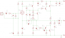
Thanks for your patience Andrew, hopefully it will be third time lucky... I feel like an idiot for messing up something so simple.
Here's the final schematic and layout. I decided to revert the bipolar input in keeping with the original TGM8 design but instead a BC546 device as a small nod to Rod's original. The JFET has its advantages, but I wasn't happy with the low gm in its degenerated state.
Gerbers available on request for anybody interested.
Attachments
Member
Joined 2009
Paid Member
Looking good boys!
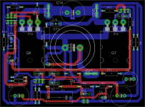
I'm wondering about some small tweaks to the pcb,
a) R18 and R19, can you use a footprint with longer leads. This will allow you to move the solder pads nearest the output further away from the power devices ? Depending on power level, it can also be convenient to use two parallel 2W resistors for each of R18 and R19 instead of one larger power device - if you have space.
b) maybe you have it already - mounting holes or clearance holes to be drilled through pcb for power devices
c) C5 shows two footprints but the far end (large size) is not connected to a trace. Neither are the other instances of the same type of footprint.
d) the 'OUT' connector, if you can, try to move it further away from the output cap as it can be fiddly to install the matching plug in a tight space
e) for C1 can you also install a footprint for a non-polar electrolytic like on TGM8 - I believe you found the sound better with the non-polar electrolytic too in your TGM8 build.
f) if you want to use a connector for the 'input' you might want to check clearance to C2, you could juggle them around for more clearance if needed (try rotating them)
Last edited:
Ah you're back! I thought you deserted us! Not sure if this is what you meant for the Re repositioning...Bigun said:Looking good boys!
I'm wondering about some small tweaks to the pcb,
a) R18 and R19, can you use a footprint with longer leads. This will allow you to move the solder pads nearest the output further away from the power devices ? Depending on power level, it can also be convenient to use two parallel 2W resistors for each of R18 and R19 instead of one larger power device - if you have space.
All you need to do is drop the flat pack part to get the drill hole in the drill file. I've put this to the test in my other projects. I've added a couple of nice tin plated holes in any case.Bigun said:b) maybe you have it already - mounting holes or clearance holes to be drilled through pcb for power devices
Bigun said:c) C5 shows two footprints but the far end (large size) is not connected to a trace. Neither are the other instances of the same type of footprint.
d) the 'OUT' connector, if you can, try to move it further away from the output cap as it can be fiddly to install the matching plug in a tight space
e) for C1 can you also install a footprint for a non-polar electrolytic like on TGM8 - I believe you found the sound better with the non-polar electrolytic too in your TGM8 build.
f) if you want to use a connector for the 'input' you might want to check clearance to C2, you could juggle them around for more clearance if needed (try rotating them)
Fixed and done. I've added a few multi-pitch options for the input cap which should satisfy any requirement!
Any other ideas? Should we add an experimental options e.g. an enhanced VAS?
Attachments
Member
Joined 2009
Paid Member
Haven't deserted you !
Not sure I can find any further suggestions:
... move the 'OUT' connector further from the big cap, just slide it south a bit")
C13 is the only SMD part shown - I never used these additional pads on the power supply for TGM8 in the end and so you may want to drop that. Or change it to a through hole, have it run north-south between the 'PWR' connector and C14 might just fit.
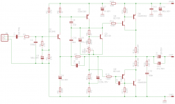
In keeping with the simple approach the enhanced VAS may not be worthwhile - I remember you found little sonic benefit? One thing you could add an option for is alternative compensation. The JLH 10W Class A classic has no Cdom and uses some other methods for compensation (cap + resistor from VAS base to ground ?).
Not sure I can find any further suggestions:
... move the 'OUT' connector further from the big cap, just slide it south a bit
C13 is the only SMD part shown - I never used these additional pads on the power supply for TGM8 in the end and so you may want to drop that. Or change it to a through hole, have it run north-south between the 'PWR' connector and C14 might just fit.
In keeping with the simple approach the enhanced VAS may not be worthwhile - I remember you found little sonic benefit? One thing you could add an option for is alternative compensation. The JLH 10W Class A classic has no Cdom and uses some other methods for compensation (cap + resistor from VAS base to ground ?).
Last edited:
Haven't deserted you !
The JLH 10W Class A classic has no Cdom and uses some other methods for compensation (cap + resistor from VAS base to ground ?).
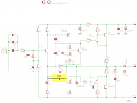
Like this?
Attachments
Hi gannaji
The resistor you have added creates nested feedback, which transfer some global negative feedback around the whole amplifier (including output stage) to local feedback around the VAS. It is a technique that Bigun used in his original TGM8 that I've chosen not to include, although I could add the pad if you are considering using my layout for your project.
The capacitor you have added is called a phase lead and is part of the compensation scheme. That extra cap you've added is actually redundant because I already included it at C15 with the proper connection to the VAS collector leg.
Attachments
In keeping with the simple approach the enhanced VAS may not be worthwhile - I remember you found little sonic benefit? One thing you could add an option for is alternative compensation. The JLH 10W Class A classic has no Cdom and uses some other methods for compensation (cap + resistor from VAS base to ground ?).
I'm inclined to agree with you that the single VAS transistor is sufficient here. The complimentary Sziklai bipolar output stage, properly biased, is already quite linear, and it will be interesting to observe what sonic influence the coupling capacitor, which is outside the feedback loop, has on an otherwise very similar version of the 'basic' TGM8, which I am intimately familiar with by now.
allow for a R+C instead of a sole C for C15.Hi gannaji
The resistor you have added creates nested feedback, which transfer some global negative feedback around the whole amplifier (including output stage) to local feedback around the VAS. It is a technique that Bigun used in his original TGM8 that I've chosen not to include, although I could add the pad if you are considering using my layout for your project.
The capacitor you have added is called a phase lead and is part of the compensation scheme. That extra cap you've added is actually redundant because I already included it at C15 with the proper connection to the VAS collector leg.
Maybe even a parallel pair of C15||(R+C) ?
Hi Ranchu,
Do add pads for the resistor. My old eyes missed C15.
About the size of the PCB: It will be ideal if it can be mounted on Heat sink of 4in by 8in, with the Power transistors below the PCB 4 inches apart. How about the output coil and Resistor in parallel?
gannaji.
Do add pads for the resistor. My old eyes missed C15.
About the size of the PCB: It will be ideal if it can be mounted on Heat sink of 4in by 8in, with the Power transistors below the PCB 4 inches apart. How about the output coil and Resistor in parallel?
gannaji.
allow for a R+C instead of a sole C for C15.
Good idea.
Hi Ranchu,
Do add pads for the resistor.
No problem
gannaji said:About the size of the PCB: It will be ideal if it can be mounted on Heat sink of 4in by 8in, with the Power transistors below the PCB 4 inches apart. How about the output coil and Resistor in parallel?
gannaji.
The printed circuit is very nearly 3x4" and is designed to be mounted to the backside of a 75mm heatsink that is popular here in Australia (Conrad Heatsinks). You will have absolutely no issues mounting two boards on your heatsink.
- Status
- This old topic is closed. If you want to reopen this topic, contact a moderator using the "Report Post" button.
- Home
- Amplifiers
- Solid State
- Bigun's TGM8 with Single Supply